
Short Answer
Definition of Dirac Cones in Two-Dimensional Materials
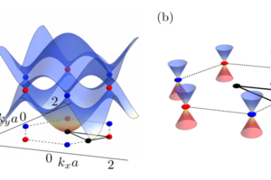
Dirac cones represent a distinctive feature in the electronic band structure of certain two-dimensional (2D) materials, where the relationship between energy and momentum forms a conical shape. This unique geometry signifies the presence of charge carriers that behave as if they are massless, enabling electrons to move through the material with minimal resistance. The phenomenon emerges from the interplay of quantum mechanics and relativistic effects, resulting in a linear energy dispersion that contrasts sharply with the typical quadratic dispersion found in conventional semiconductors.
- Dirac cones:
Conical intersections in the band structure where conduction and valence bands meet at discrete points, leading to massless charge carriers. - Massless charge carriers:
Electrons or holes that exhibit linear dispersion and behave as relativistic particles with zero effective mass. - Linear dispersion relation:
Energy varies linearly with momentum near the Dirac points, unlike the parabolic dispersion in ordinary materials.
Bismuth-Antimony Thin Films: A Platform for Dirac Physics
Bismuth-antimony (Bi-Sb) alloys, known for their narrow bandgap semimetallic nature, have attracted considerable attention due to their intriguing electronic characteristics. When fabricated as thin films, Bi-Sb exhibits enhanced quantum effects that can give rise to novel physical phenomena, including the formation of Dirac cones. The crystal structure of Bi-Sb is inherently non-centrosymmetric, which induces strong spin-orbit coupling-a critical factor that intertwines an electron’s spin with its momentum. This coupling facilitates the emergence of topological states, some of which are directly linked to Dirac cone formation.
Quantum Confinement and Thickness Dependence
Reducing Bi-Sb to ultrathin layers introduces quantum confinement effects that significantly alter its electronic properties. Variations in film thickness modulate the density of states and electronic band structure, enabling precise control over conductivity and the manifestation of Dirac physics. This tunability makes Bi-Sb thin films an ideal system for investigating how dimensional constraints influence electronic behavior.
Mechanisms Underlying Dirac Cone Formation in Bi-Sb Films
The emergence of Dirac cones in Bi-Sb thin films is primarily driven by the synergy between spin-orbit coupling and the material’s crystalline symmetry. The strong spin-orbit interaction lifts degeneracies in the band structure, while the lack of inversion symmetry allows for topologically nontrivial states to develop. These states are characterized by robust surface conduction channels protected by topological invariants, which are mathematical quantities that remain unchanged under continuous deformations of the system.
Influence of External Factors on Dirac Cone Stability
Several external parameters critically affect the behavior and stability of Dirac cones in Bi-Sb thin films:
- Temperature:
Thermal fluctuations can induce phonon interactions that disrupt the delicate balance maintaining Dirac cones, potentially altering electronic transport properties. - Magnetic Fields:
Magnetic ordering can modify the Dirac cone structure, leading to phenomena such as quantum Hall effects and spin textures, which are pivotal for spintronic applications. - Film Thickness:
Changes in thickness influence quantum confinement, thereby tuning the electronic band structure and the presence of Dirac cones.
Experimental Techniques for Probing Dirac Cones
Advanced characterization methods are essential for investigating the electronic structure of Bi-Sb thin films. Angle-resolved photoemission spectroscopy (ARPES) is a powerful tool that maps the energy-momentum relationship of electrons, providing direct evidence of Dirac cones and topologically protected surface states. These experimental insights are supported by theoretical models based on topological invariants, bridging the gap between abstract theory and observable phenomena.
Applications and Technological Significance
The unique electronic properties of Dirac cones in Bi-Sb thin films hold promise for a variety of cutting-edge technologies. Their massless charge carriers and topologically protected states could enable the development of low-power electronic devices, high-speed transistors, and components for quantum computing. Moreover, the interplay between magnetism and Dirac physics opens avenues for spintronics, where electron spin is exploited for information processing, potentially revolutionizing data storage and transfer technologies.
Challenges in Realizing Practical Bi-Sb Dirac Materials
Despite the exciting prospects, several obstacles remain in harnessing Dirac cones within Bi-Sb thin films for practical use. Achieving high crystalline quality, minimizing impurities, and developing reliable fabrication methods are critical challenges. Balancing the preservation of intrinsic Dirac physics with the demands of material stability and scalability requires ongoing research and innovation.
Summary and Future Outlook
The study of Dirac cones in bismuth-antimony thin films represents a vibrant intersection of fundamental physics and applied materials science. This research not only deepens our understanding of electron dynamics in reduced dimensions but also paves the way for transformative technological advancements. As experimental techniques and theoretical models continue to evolve, the exploration of these exotic electronic states promises to unlock new frontiers in condensed matter physics and device engineering.
FAQ
What are Dirac cones?
Dirac cones are features in the electronic band structure of certain materials where charge carriers behave as massless particles.
Why are bismuth-antimony thin films significant?
They exhibit unique electronic properties, including the formation of Dirac cones, making them promising for advanced technologies.
What factors influence Dirac cone stability?
Temperature, magnetic fields, and film thickness can critically affect the behavior and stability of Dirac cones.


Leave a Reply