Short Answer
Definition of Semiconductors and Their Role
Semiconductors are materials that possess electrical conductivity between that of conductors and insulators, making them essential components in modern electronics. They serve as the fundamental building blocks for digital devices by controlling the flow of electrical current through their unique electronic properties. Common semiconductor materials include silicon and germanium, which have specific energy bandgaps enabling the regulation of electrical conductivity.
Limitations of Traditional Semiconductor Materials
Despite their widespread use, conventional semiconductors face inherent challenges. These include issues with thermal dissipation, which limits their performance at elevated temperatures, and reduced efficiency when operating at high frequencies. Such constraints become increasingly apparent as emerging technologies like artificial intelligence, the Internet of Things (IoT), and large-scale data processing demand more from semiconductor devices.
Exploring Advanced Crystalline Materials
To overcome these limitations, researchers are investigating alternative crystalline materials with superior electronic and thermal properties. The atomic arrangement within these crystals plays a crucial role in enhancing semiconductor performance beyond what traditional materials can offer.
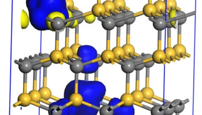
Group IV Semiconductors
Materials such as silicon carbide (SiC) and gallium nitride (GaN), belonging to the group IV semiconductor family, have attracted significant interest. These compounds exhibit excellent thermal conductivity, making them suitable for high-temperature and high-power applications. However, integrating these materials into existing manufacturing workflows presents challenges, especially as the demand for energy-efficient electronics grows.
Two-Dimensional (2D) Materials
Advancements in material science have introduced two-dimensional crystals like graphene and transition metal dichalcogenides (TMDs), which offer promising avenues for next-generation semiconductors.
- Graphene:
Composed of a single layer of carbon atoms arranged in a hexagonal lattice, graphene boasts exceptional electrical conductivity and mechanical strength. Despite these advantages, its lack of an intrinsic bandgap limits its direct application in digital electronics where switching behavior is essential. - Transition Metal Dichalcogenides (TMDs):
Materials such as molybdenum disulfide (MoS2) possess direct bandgaps, making them attractive candidates for transistor technology. However, challenges remain in synthesizing these materials with the precision and scalability required for commercial semiconductor manufacturing.
Techniques for Synthesizing High-Quality Crystals
The fabrication of superior semiconductor crystals relies on advanced synthesis methods that ensure precise atomic arrangements. Two prominent techniques include:
- Chemical Vapor Deposition (CVD):
A process where gaseous reactants form solid crystalline layers on substrates, enabling controlled growth of thin films. - Molecular Beam Epitaxy (MBE):
A highly controlled method that deposits atomic layers under ultra-high vacuum conditions, allowing for exceptional crystal quality.
While these methods produce high-purity crystals, scaling them economically for industrial production remains a significant hurdle, creating a balance between quality and cost-effectiveness.
Heterostructure Engineering and Composite Crystals
Combining different semiconductor materials at the atomic level through heterostructure engineering offers a pathway to tailor electronic properties. By stacking or integrating dissimilar crystals, it is possible to harness the best attributes of each component, potentially leading to devices with unprecedented performance.
However, ensuring lattice compatibility between different materials is a complex challenge. Mismatches can introduce defects or strain, which may degrade device performance, necessitating innovative approaches in material design and synthesis.
The Role of Defects in Semiconductor Crystals
Traditionally, defects within crystal lattices have been viewed as detrimental to semiconductor performance. Recent studies, however, suggest that certain defects can be beneficial, especially in ultra-wide bandgap semiconductors, by enabling new functionalities and enhancing device characteristics.
This evolving understanding prompts a shift towards defect engineering, where controlled introduction and manipulation of imperfections can fine-tune electronic properties rather than simply aiming for perfect crystal purity.
Interdisciplinary Collaboration in Semiconductor Research
Advancing the field of crystalline semiconductors requires a multidisciplinary approach, integrating insights from physics, materials science, and engineering. Such collaboration is vital to unravel the complexities of crystal behavior and to develop innovative solutions that push the boundaries of semiconductor technology.
Why Crystalline Semiconductors Are Crucial for the Future
The exploration of crystalline structures as a foundation for next-generation semiconductors holds immense promise. By integrating novel materials, refining synthesis techniques, and leveraging defect engineering, the semiconductor industry can achieve breakthroughs in manufacturing efficiency, energy consumption, and computational power.
As digital technologies continue to evolve rapidly, harnessing the unique properties of crystalline materials will be key to overcoming current limitations and ushering in a new era of electronic devices with enhanced capabilities.
FAQ
What are semiconductors?
Semiconductors are materials with electrical conductivity between that of conductors and insulators, used in electronics to control electrical current.
Why are crystalline materials important for semiconductors?
Crystalline materials offer superior electronic and thermal properties, which can overcome limitations of traditional semiconductor materials.
What are some advanced synthesis techniques for crystals?
Techniques like Chemical Vapor Deposition (CVD) and Molecular Beam Epitaxy (MBE) are used to produce high-quality semiconductor crystals.


Leave a Reply