Short Answer
Definition of Boron in Semiconductor Context
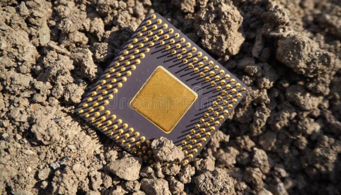
Boron, traditionally known for its applications in agriculture and chemistry, is increasingly being investigated as a potential semiconductor material. Semiconductors are materials with electrical conductivity that lies between conductors and insulators, primarily determined by their electronic band structure. This includes a valence band filled with bonding electrons and a conduction band where free electrons enable electrical conduction. The energy difference between these bands, known as the bandgap, is crucial in defining semiconductor behavior. Typically, semiconductors have a bandgap that allows electrons to be thermally excited or manipulated through doping to conduct electricity.
Electronic Properties of Boron
Boron exhibits distinctive electronic characteristics depending on its allotrope. In its crystalline form, boron is renowned for its hardness and structural robustness, featuring a diamond-like lattice with strong covalent bonds. This bonding arrangement results in a complex band structure with an indirect bandgap of about 0.4 eV, which is relatively narrow compared to conventional semiconductors. Although boron itself does not fully meet the standard criteria of a semiconductor, its near-semiconductor properties have sparked interest in its potential applications within semiconductor technology.
Boron as a Dopant in Semiconductor Materials
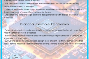
One of the most significant roles of boron in semiconductor physics is its function as a dopant. When introduced into silicon, boron acts as a p-type dopant by creating “holes” or positive charge carriers in the silicon lattice. This modification enhances the electrical conductivity of silicon by facilitating hole conduction, which is essential for forming p-n junctions-the fundamental building blocks of many electronic devices. The interaction between boron and traditional semiconductor materials like silicon opens pathways for optimizing device performance and expanding the functionality of existing semiconductor platforms.
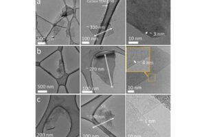
Advancements in Boron Nanostructures
Recent progress in nanotechnology has revealed that boron-based nanostructures, including boron nanotubes and boron nitride, possess remarkable electrical, thermal, and chemical properties. These nanomaterials demonstrate exceptional stability and unique electronic behaviors that could potentially compete with or complement traditional semiconductor materials. Although fabricating and manipulating these nanostructures require sophisticated techniques, their promising attributes make them attractive candidates for future applications in electronics, photonics, and energy devices such as photovoltaics.
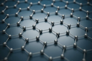
Boron in Emerging Two-Dimensional Semiconductor Materials
The exploration of two-dimensional (2D) materials, such as graphene and transition metal dichalcogenides, has expanded to include boron-doped variants. Incorporating boron into these 2D materials has been shown to enhance charge carrier mobility and introduce novel photonic properties. These improvements could lead to the development of next-generation optoelectronic devices characterized by faster data processing capabilities and reduced energy consumption. Such innovations are critical for advancing modern technology and meeting the increasing demands for efficient electronic components.
Challenges in Boron Semiconductor Integration
Despite its potential, several obstacles hinder the widespread adoption of boron in semiconductor applications. Producing high-purity boron and refining doping techniques remain areas requiring extensive research. Additionally, ensuring the stability and scalability of boron-based materials is essential for their practical use in industry. Integrating boron into existing semiconductor manufacturing processes may also necessitate significant innovations in fabrication methods, as the semiconductor industry demands materials that meet rigorous performance and reliability standards.
Environmental and Sustainability Considerations
From an ecological standpoint, boron offers advantages due to its relative abundance compared to other semiconductor elements, which are often scarce or environmentally taxing to extract. Utilizing boron in semiconductor devices could contribute to more sustainable electronics manufacturing, aligning with global initiatives to minimize the environmental footprint of technology production. This perspective underscores the importance of interdisciplinary collaboration among materials science, electrical engineering, and environmental research to develop greener semiconductor solutions.
Conclusion: The Future of Boron in Semiconductor Technology
While boron does not currently fulfill all traditional semiconductor criteria, its unique properties as a dopant and within novel nanostructures present exciting opportunities for future exploration. The integration of boron into semiconductor technologies represents a promising frontier that encourages innovation and interdisciplinary research. As the demand for more efficient, sustainable, and advanced electronic devices grows, boron’s evolving role in semiconductor physics exemplifies the dynamic nature of materials science and the ongoing quest to redefine technological possibilities.
FAQ
Is boron a semiconductor?
Boron itself is not a conventional semiconductor but exhibits unique electronic properties with a small indirect bandgap. It is used primarily as a p-type dopant in silicon semiconductors and shows promise in boron-based nanostructures.
What role does boron play in semiconductor technology?
Boron acts as a p-type dopant in silicon, creating holes that enhance electrical conduction. It is also studied for its unique properties in boron nanotubes and boron nitride nanostructures.
What are the challenges in using boron as a semiconductor material?
Challenges include synthesizing high-purity boron, developing effective doping techniques, ensuring material stability, scalability, and integrating boron into existing semiconductor manufacturing processes.
Why is boron considered promising for future semiconductor applications?
Due to its abundance, potential for sustainability, and unique electronic and thermal properties in nanostructured forms, boron is considered promising for next-generation semiconductor devices.


Leave a Reply