Short Answer
Definition of Atom Lithography
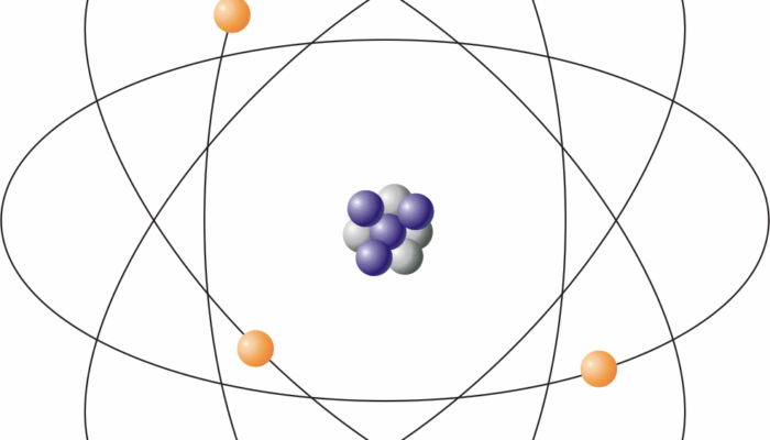
Atom lithography is an advanced fabrication technique that utilizes individual atoms as the fundamental units for creating highly detailed structures at the nanoscale. Unlike traditional lithographic methods that employ light or electrons to pattern surfaces, atom lithography harnesses the unique quantum properties of atoms to achieve unprecedented precision in material manipulation. This method enables the construction of devices and materials with atomic-level accuracy, opening new frontiers in nanotechnology and materials science.
Fundamental Principles Behind Atom Lithography
The core mechanism of atom lithography is based on the wave-particle duality inherent to atoms. Atoms behave both as discrete particles and as waves, allowing scientists to exploit quantum phenomena such as interference and diffraction to control their trajectories. By directing a beam of atoms onto a substrate with extreme precision, it becomes possible to “print” atomically thin layers or patterns. This quantum control surpasses the resolution limits of conventional photolithography, which is constrained by the wavelength of light.
Quantum Properties Utilized
- Wave-Particle Duality:
Atoms exhibit wave-like behavior, enabling manipulation through interference patterns. - Diffraction and Interference:
These phenomena allow the focusing and shaping of atomic beams to form nanoscale patterns.
Comparison with Traditional Lithography Techniques
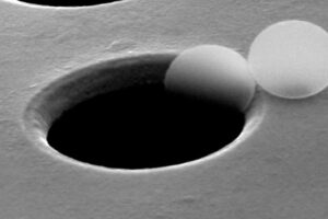
Traditional lithography, such as photolithography, relies on light to transfer patterns onto substrates, typically limited by the diffraction limit of light wavelengths. Electron beam lithography improves resolution but still faces challenges at the atomic scale. Atom lithography, by contrast, uses the atoms themselves as the “ink,” allowing for patterning at scales on the order of 0.1 nanometers, which is the approximate size of an atom. This fundamental difference enables the fabrication of structures with atomic precision, unattainable by other methods.
Technical Challenges and Scalability
Despite its remarkable precision, atom lithography faces significant hurdles before it can be adopted for large-scale manufacturing. Current implementations are primarily confined to research environments due to difficulties in maintaining stable atomic beams, controlling atom-surface interactions, and mitigating environmental disturbances such as quantum decoherence and atomic scattering. Scaling this technology to industrial levels requires overcoming these obstacles through innovative engineering and interdisciplinary collaboration.
Key Technical Issues
- Beam Stability:
Maintaining a consistent and focused atomic beam is critical for precise patterning. - Surface Interactions:
Understanding and controlling how atoms interact with substrates affects pattern fidelity. - Environmental Factors:
Quantum decoherence and scattering can degrade the quality of atomic patterns.
Applications Across Various Fields
Atom lithography holds transformative potential in multiple domains, including electronics, photonics, and quantum computing. In electronics, it enables the fabrication of transistors and circuits at atomic scales, potentially leading to devices with enhanced speed and energy efficiency. In quantum computing, atom lithography can be instrumental in creating qubits-the fundamental units of quantum information-thereby advancing the development of powerful quantum processors. Additionally, the technique allows for the engineering of materials with customized electrical, optical, and mechanical properties by precisely controlling atomic arrangements.
Examples of Practical Use
- Atomic-Scale Transistors:
Creating ultra-small transistors that improve device performance and reduce power consumption. - Quantum Bits (Qubits):
Fabricating qubits with atomic precision to enhance quantum computing capabilities. - Tailored Nanomaterials:
Designing materials with specific properties for use in sensors, photonic devices, and more.
Interrelation Between Atomic Structure and Material Properties
The atomic configuration within a material fundamentally influences its physical characteristics, including electrical conductivity, optical behavior, and mechanical strength. Atom lithography offers the ability to engineer these configurations with exceptional control, enabling the creation of bespoke materials tailored for specialized applications. Achieving this level of precision requires a deep understanding of both quantum mechanics and material science, highlighting the interdisciplinary nature of this technology.
Ethical and Societal Considerations
As atom lithography advances, it raises important ethical questions regarding the responsible use of such powerful technology. The capability to manipulate matter at the atomic scale could lead to revolutionary benefits but also poses risks related to equitable access, environmental impact, and potential misuse. It is essential to establish guidelines and safeguards to ensure that the development and deployment of atom lithography serve the broader interests of society and promote fairness in technological advancement.
Key Ethical Questions
- Access and Equity:
How can we ensure that the benefits of atom lithography are distributed fairly across different populations? - Regulation and Safety:
What measures are necessary to prevent misuse and manage environmental impacts? - Long-Term Implications:
How will this technology affect societal structures and economic systems?
Future Outlook and Importance
Atom lithography represents a paradigm shift in material fabrication, with the potential to revolutionize technology by enabling atomic-scale engineering. Its impact could extend across scientific research, industrial manufacturing, and emerging technologies such as quantum computing. However, realizing this potential depends on addressing technical challenges, fostering interdisciplinary collaboration, and navigating ethical considerations. As research progresses, atom lithography is poised to become a cornerstone of next-generation nanotechnology, shaping the future of engineering and material science.
FAQ
What is atom lithography?
Atom lithography is an advanced fabrication technique that utilizes individual atoms for creating highly detailed structures at the nanoscale.
How does atom lithography differ from traditional lithography?
Unlike traditional methods that use light or electrons, atom lithography uses atoms themselves, allowing for unprecedented precision down to 0.1 nanometers.
What are the applications of atom lithography?
Applications include the fabrication of atomic-scale transistors, qubits for quantum computing, and tailored nanomaterials.


Leave a Reply