Short Answer
Definition of Two-Dimensional Atomic Crystals
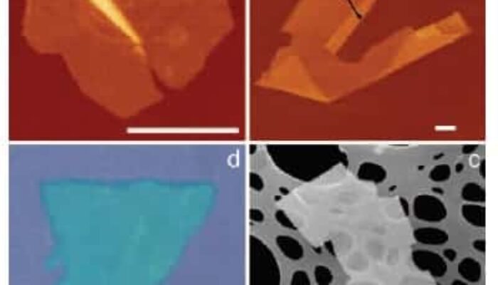
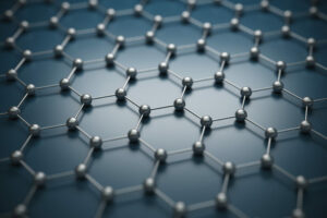
Two-dimensional (2D) atomic crystals are materials consisting of a single or few layers of atoms arranged in a planar lattice. Unlike their three-dimensional (3D) counterparts, these crystals exhibit unique physical and chemical characteristics due to their reduced dimensionality. Prominent examples include graphene, molybdenum disulfide (MoS2), and hexagonal boron nitride (h-BN), which have become central to modern condensed matter physics research.
- Graphene:
A single layer of carbon atoms arranged in a hexagonal lattice, known for its exceptional electrical conductivity and mechanical strength. - Molybdenum Disulfide (MoS2):
A semiconducting 2D material with promising applications in electronics and photonics. - Hexagonal Boron Nitride (h-BN):
An insulating 2D crystal often used as a substrate or protective layer in device fabrication.
Fundamental Properties and Electronic Structure
The transition from bulk 3D materials to atomically thin 2D layers profoundly alters their electronic band structures. In bulk solids, electronic states are influenced by interlayer coupling, whereas in 2D crystals, the absence of such interactions leads to distinct bandgap characteristics. This bandgap can be dynamically tuned by external factors such as mechanical strain or electrostatic gating, enabling precise control over the material’s electronic behavior.
Moreover, the unique lattice symmetry and reduced dimensionality give rise to novel quantum phenomena, including quantum tunneling and the quantum Hall effect, which have been experimentally observed in these materials. When doped appropriately, some 2D crystals even exhibit superconductivity at relatively elevated temperatures, highlighting their potential for quantum device applications.
Phonon Dynamics and Thermal Properties
Phonons, the quantized vibrational modes of a crystal lattice, behave differently in 2D materials compared to their 3D analogs. The phonon dispersion relations in monolayer crystals show the absence or modification of certain vibrational modes, such as out-of-plane optical phonons in graphene. This alteration significantly impacts thermal conductivity and heat transport mechanisms, making 2D materials attractive for thermal management and thermoelectric applications.
Applications in Electronics and Photonics
The exceptional electrical and optical properties of 2D atomic crystals have spurred their integration into next-generation technologies. Graphene’s high carrier mobility makes it ideal for high-speed transistors and transparent conductive films. Meanwhile, the semiconducting nature of MoS2 enables its use in photodetectors and flexible electronics, where traditional materials fall short.
Additionally, stacking different 2D materials to form van der Waals heterostructures creates new functionalities not present in individual layers. These heterostructures combine diverse electronic and optical properties, paving the way for multifunctional devices with tailored characteristics.
Challenges in Stability and Scalability
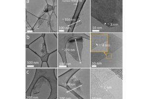
Despite their promising attributes, 2D atomic crystals face significant hurdles related to environmental stability and large-scale production. Their atomically thin nature makes them vulnerable to degradation from moisture, oxygen, and other environmental factors. Protective encapsulation and coating techniques are essential to preserve their properties in practical devices.
Furthermore, synthesizing high-quality monolayers consistently and economically remains a challenge. Techniques such as chemical vapor deposition (CVD) and liquid-phase exfoliation are under continuous development to meet industrial demands for scalable and reproducible 2D material fabrication.
Energy Storage and Biomedical Prospects
Beyond electronics, 2D materials are gaining traction in energy-related applications. Their high surface area and unique electrochemical properties enhance ion adsorption and charge transfer, making them excellent candidates for lithium-ion batteries and supercapacitors. In biomedicine, interactions between 2D crystals and biological systems have opened new avenues for drug delivery platforms and sensitive biosensors, demonstrating their versatility across disciplines.
Common Misconceptions About 2D Materials
2D materials are just thinner versions of bulk materials.
The reduction to two dimensions fundamentally changes their electronic, optical, and mechanical properties, often resulting in entirely new phenomena.
All 2D materials are conductive like graphene.
While graphene is highly conductive, other 2D materials such as MoS2 are semiconductors, and h-BN is an insulator, illustrating a wide range of electronic behaviors.
Significance and Future Outlook
The discovery and exploration of 2D atomic crystals represent a transformative chapter in materials science and condensed matter physics. Their unique properties challenge traditional paradigms and offer unprecedented opportunities for innovation in electronics, photonics, energy, and quantum technologies. As research advances, the integration of 2D materials into commercial applications promises to revolutionize multiple industries, underscoring their critical role in shaping future technological landscapes.
FAQ
What are 2D atomic crystals?
Materials consisting of single or few layers of atoms that exhibit unique properties compared to their 3D counterparts.
What are some applications of 2D materials?
They are used in electronics for high-speed transistors, photodetectors, energy storage devices, and biomedical applications.
What challenges do 2D atomic crystals face?
Challenges include environmental stability and scalability in production methods.


Leave a Reply