
Short Answer
Definition of Two-Dimensional Materials
Two-dimensional (2D) materials are crystalline substances consisting of a single layer of atoms, exhibiting unique physical and chemical properties distinct from their bulk counterparts. Their atomic-scale thickness imparts exceptional characteristics that have attracted significant attention in scientific research and technological development.
- Atomic Thinness:
2D materials are composed of one or a few atomic layers, resulting in ultra-thin structures with high surface area-to-volume ratios. - Examples:
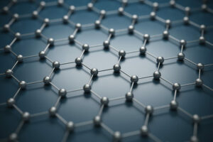
Graphene, a single layer of carbon atoms arranged in a hexagonal lattice, is the most renowned 2D material. Others include transition metal dichalcogenides (TMDs) like molybdenum disulfide (MoS2), which exhibit semiconducting properties.
Fundamental Properties and Mechanisms
The distinctive features of 2D materials arise from their reduced dimensionality, which influences their mechanical, electrical, thermal, and optical behaviors.
- Mechanical Strength and Flexibility:
The atomic thinness grants 2D materials remarkable flexibility and tensile strength, making them ideal for flexible electronics. - Electrical Conductivity:
Graphene, for instance, demonstrates extraordinary electrical conductivity due to its delocalized π-electrons, facilitating rapid electron transport. - Quantum Confinement Effects:
In materials like TMDs, electrons are confined within two dimensions, leading to tunable bandgaps and unique optical properties beneficial for photonic devices. - Thermal Conductivity:
Many 2D materials exhibit high thermal conductivity, enabling efficient heat dissipation in nanoelectronic applications.
Applications and Technological Implications
The exceptional properties of 2D materials have paved the way for innovations across multiple sectors, including electronics, energy, and photonics.
- Nanoelectronics:
The miniaturization potential of 2D materials supports the development of ultra-thin, high-performance electronic components. - Energy Storage and Conversion:
Their high surface area and charge carrier mobility enhance the efficiency of batteries, supercapacitors, and photovoltaic cells. - Optoelectronics:
Tunable bandgaps in TMDs enable their use in light-emitting diodes, photodetectors, and other photonic devices. - Heterostructures:
Stacking different 2D layers creates composite materials with customizable properties, expanding the scope of device engineering.
Challenges in Synthesis and Scalability
Despite their promising attributes, 2D materials face significant obstacles related to their production and practical deployment.
- Scalability Issues:
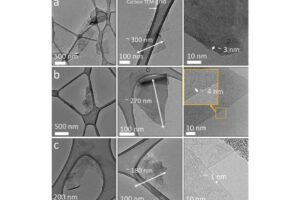
Common fabrication methods such as mechanical exfoliation and chemical vapor deposition (CVD) often lack the efficiency and cost-effectiveness required for mass production. - Complexity of Manufacturing:
Achieving uniformity and high quality at large scales remains a technical challenge, impeding industrial adoption. - Potential Solutions:
Advances in synthesis techniques and automation may help bridge the gap between laboratory research and commercial manufacturing.
Stability and Environmental Sensitivity
The long-term performance of 2D materials is influenced by their interaction with environmental factors, which can degrade their properties over time.
- Degradation Mechanisms:
Exposure to oxygen, moisture, and other ambient conditions can alter the chemical and electronic structure of materials like graphene oxide. - Impact on Performance:
Such degradation affects conductivity, mechanical integrity, and overall device reliability. - Enhancing Durability:
Protective coatings, chemical modifications, and encapsulation strategies are being explored to improve stability without sacrificing functionality.
Defect Engineering and Material Quality
Defects within 2D materials play a dual role, sometimes enhancing and other times impairing their intrinsic properties.
- Beneficial Defects:
Certain imperfections can introduce desirable electronic states or catalytic activity. - Detrimental Defects:
Uncontrolled defects often degrade electrical conductivity and mechanical strength. - Control Strategies:
Precise fabrication and post-synthesis treatments are essential to manage defect density and distribution.
Integration with Existing Technologies
Incorporating 2D materials into conventional devices presents compatibility challenges due to their unique physical and chemical characteristics.
- Material Hybridization:
Combining 2D layers with bulk substrates requires innovative assembly techniques to maintain interface integrity. - Device Architecture:
Traditional electronic designs may need adaptation to fully exploit the advantages of 2D materials. - Research Directions:
Developing scalable integration methods is critical for transitioning 2D materials from research to practical applications.
Future Prospects and Innovations
Ongoing research continues to expand the potential of 2D materials, exploring novel structures and applications.
- Nanostructuring:
Tailoring the morphology and composition at the nanoscale enables customization of material properties. - Heterostructure Engineering:
Layering different 2D materials creates multifunctional composites with synergistic effects. - Energy Applications:
Enhanced charge transport and surface reactivity position 2D materials as key components in next-generation energy devices.
Common Misconceptions About 2D Materials
2D materials are universally stable under all conditions.
Many 2D materials are sensitive to environmental factors and require protective measures to maintain performance.
Large-scale production of 2D materials is already commercially viable.
Current synthesis methods face scalability and cost challenges that limit widespread industrial use.
Defects always degrade material properties.
Some defects can enhance specific functionalities, making defect engineering a valuable tool.
Significance of 2D Materials in Science and Technology
The exploration of 2D materials represents a transformative frontier in material science, with profound implications for future technologies. Their exceptional properties enable advancements in electronics, energy storage, and photonics, potentially revolutionizing industries and contributing to sustainable development. Understanding and overcoming the challenges associated with their synthesis, stability, and integration are essential steps toward harnessing their full potential in practical applications.
FAQ
What are two-dimensional materials?
Two-dimensional materials are crystalline substances consisting of a single layer of atoms, exhibiting unique physical and chemical properties.
What are some applications of 2D materials?
2D materials are used in nanoelectronics, energy storage, optoelectronics, and the creation of heterostructures.
What challenges do 2D materials face?
Challenges include scalability issues, complexity of manufacturing, and environmental sensitivity affecting their stability.


Leave a Reply