Short Answer
Definition of Nanoribbons and Ballistic Electrons
Nanoribbons are ultra-thin strips of material, often derived from two-dimensional substances like graphene, that exhibit unique electrical and physical properties at the nanoscale. These structures have become pivotal in advancing nanoscale physics, particularly in the study of electron conduction. A key concept related to electron transport in these materials is that of ballistic electrons. Ballistic electrons are charge carriers that traverse a medium while preserving their energy and momentum, encountering minimal scattering or resistance-much like a projectile moving through air with negligible friction.
- Nanoribbons:
Narrow, ribbon-like nanostructures typically fabricated from graphene or similar 2D materials, characterized by their exceptional electrical conductivity and tunable properties. - Ballistic Electrons:
Electrons that move through a conductor without scattering, maintaining coherent motion over relatively long distances at the nanoscale.
Fundamentals of Ballistic Electron Transport
In conventional conductors, electrons frequently collide with impurities, lattice vibrations (phonons), and other electrons, resulting in resistance and energy dissipation. However, in nanoribbons, especially those made from high-quality graphene, electrons can travel ballistically over distances that can reach several micrometers. This phenomenon is rooted in quantum mechanics, where the wave-like nature of electrons and the reduced dimensionality of the material suppress scattering events. The degree of ballistic transport depends on factors such as material purity, temperature, and structural dimensions.
Structural Influence on Electron Mobility in Graphene Nanoribbons
Graphene nanoribbons (GNRs) exemplify the interplay between structure and electron transport. The honeycomb lattice of carbon atoms in graphene provides an inherently high electron mobility. When graphene is patterned into nanoribbons, the width and edge configuration critically influence electronic behavior:
- Quantum Confinement:
Narrower ribbons exhibit pronounced quantum confinement effects, altering the electronic band structure and enabling discrete energy levels. - Classical Behavior:
Wider ribbons tend to behave more like bulk graphene, with electron transport resembling classical conduction.
This tunability allows for the engineering of GNRs with tailored electronic properties suitable for specific technological applications.
Applications Leveraging Ballistic Transport in Nanoribbons
The unique ability of electrons to move ballistically in nanoribbons opens avenues for innovative electronic and quantum devices:
- Field-Effect Transistors (FETs):
Ballistic conduction enables faster switching speeds and lower power consumption, enhancing device efficiency. - Sensors:
High sensitivity and rapid response times are achievable due to minimal electron scattering. - Quantum Computing Components:
Preservation of quantum coherence over longer distances supports the development of quantum information technologies.
Challenges Affecting Ballistic Electron Travel
Despite the promising theoretical framework, several practical obstacles limit the full realization of ballistic transport in nanoribbons:
- Temperature Effects:
Elevated temperatures increase phonon activity, which enhances electron scattering and reduces ballistic transport distances. - Material Quality:
Defects, impurities, and edge irregularities serve as scattering centers, diminishing electron mobility. - Fabrication Limitations:
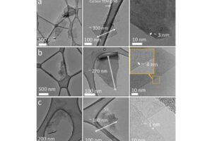
Producing nanoribbons with consistent high purity and precise dimensions remains technologically challenging, with methods like chemical vapor deposition (CVD) and liquid-phase exfoliation still facing scalability and reproducibility issues.
Dimensionality and Quantum Effects in Nanoribbons
The one-dimensional nature of nanoribbons introduces distinct quantum phenomena that influence electron transport. Theories of 1D conductors predict unique electrical characteristics, such as quantized conductance and enhanced electron coherence, which are pivotal for developing ultrafast electronic and photonic devices. However, maintaining stability and performance in practical environments requires further research and innovation.
Interdisciplinary Approaches to Overcome Limitations
Addressing the challenges in ballistic electron transport necessitates a multidisciplinary strategy combining material science, physics, and engineering. Emerging research focuses on hybrid systems that integrate nanoribbons with other materials to enhance performance. Advances in nanofabrication and in-situ characterization techniques are enabling unprecedented control over electron pathways, fostering new possibilities for device design and functionality.
Significance of Ballistic Electron Transport in Nanoribbons
The study of how far ballistic electrons can travel within nanoribbons represents a critical intersection of multiple scientific fields. Understanding and harnessing this phenomenon promises transformative impacts on nanotechnology and electronics, potentially leading to faster, more efficient devices and novel quantum technologies. While challenges remain, the pursuit of mastering ballistic transport continues to inspire innovation and expand the frontiers of nanoscale science.
FAQ
What is ballistic electron transport?
It is a mode of electron conduction where electrons travel through a material with minimal scattering, maintaining their energy and momentum.
Why are nanoribbons significant in electron transport studies?
Their low-dimensional structure reduces scattering, allowing for ballistic transport and quantum confinement effects that can be engineered.
What challenges exist in utilizing ballistic transport in devices?
Maintaining material purity, controlling temperature effects, and fabricating defect-free nanoribbons are major challenges.


Leave a Reply