Short Answer
Definition of Excitonic Integrated Circuits
Excitonic integrated circuits (EICs) represent an emerging frontier in optoelectronics, blending the principles of photonics and electronics by utilizing light-based particles rather than solely relying on electron flow for information transmission and processing. Central to these circuits are excitons-quasi-particles formed by the coupling of an electron and a hole within a semiconductor. These bound states exhibit distinctive quantum mechanical properties that enable innovative functionalities in electronic and photonic devices.
Fundamentals of Excitons
An exciton is created when a photon excites an electron from the valence band to the conduction band of a semiconductor, leaving behind a positively charged hole. The electron and hole attract each other through Coulomb forces, forming a bound pair known as an exciton. Excitons can be categorized as either direct or indirect:
- Direct excitons:
These have the electron and hole located in the same spatial region, resulting in higher mobility and reduced scattering losses. - Indirect excitons:
Here, the electron and hole are separated spatially, which typically leads to longer lifetimes but lower mobility.
The unique light-matter interaction capabilities of excitons make them highly suitable for applications requiring rapid data processing and energy-efficient operation.
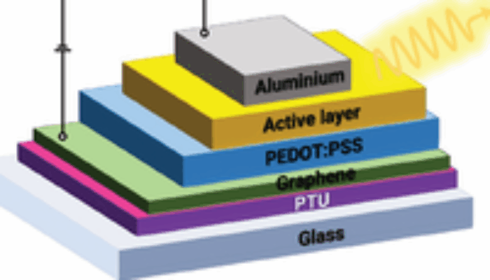
Materials for Exciton Generation and Manipulation
Various advanced materials have been explored to optimize exciton creation and control, including:
- Transition Metal Dichalcogenides (TMDs):
Atomically thin semiconductors like molybdenum disulfide (MoS2) exhibit strong excitonic effects even at room temperature, making them ideal for practical EIC applications. - Perovskites:
These materials offer excellent light absorption and exciton binding energies, contributing to efficient exciton dynamics. - Organic Semiconductors:
Known for their flexibility and tunable properties, organic materials provide alternative platforms for exciton-based devices.
Architectural Designs of Excitonic Integrated Circuits
The structural design of EICs is complex and multifaceted, incorporating several innovative approaches to optimize exciton behavior:
- Waveguide-Based Architectures:
These systems guide excitons along predefined paths, enhancing their interactions through engineered dielectric environments. - Coupled Excitonic Systems:
Multiple excitonic states interact within these configurations, enabling advanced functionalities such as coherent exciton transport. - Nanophotonic Hybrid Structures:
Integration of nanophotonic elements with excitonic materials creates hybrid platforms that exploit phenomena like slow light and superradiance for improved information storage and transmission.
Role of Photonic Bandgap and Nanostructuring
Photonic bandgap engineering plays a crucial role in controlling exciton dynamics within EICs. By designing periodic nanostructures, it is possible to manipulate exciton propagation and minimize energy losses. Additionally, nanoscale lattice tailoring enhances exciton confinement and guiding capabilities, addressing challenges such as thermal dissipation and signal degradation. These advancements contribute to the overall efficiency and stability of excitonic circuits.
Integration with Conventional Electronics
Combining excitonic circuits with traditional electronic components opens avenues for multifunctional devices. Hybrid systems that merge electronic transistors with photonic excitonic elements enable seamless data conversion and transfer between electronic and photonic domains. This synergy is essential for developing ultra-fast, low-power computing architectures that transcend the limitations of purely electronic systems.
Applications of Excitonic Integrated Circuits
EICs hold transformative potential across various technological sectors:
- Telecommunications:
By exploiting exciton-polariton phenomena, EICs can facilitate devices operating at exceptionally high bandwidths, meeting the growing demand for rapid and efficient data transmission. - Data Processing:
The enhanced light-matter interactions in excitonic circuits promise faster and more energy-efficient computational processes. - Sensing Technologies:
Exciton-based sensors can detect subtle environmental changes such as temperature, pressure, and chemical composition with high sensitivity. Their integration into wearable devices could enable real-time health monitoring and responsive feedback systems.
Challenges in Excitonic Circuit Development
Despite their promise, several obstacles must be overcome to realize practical EICs:
- Exciton Stability:
Excitons typically have short lifetimes due to nonradiative recombination, necessitating the development of materials that can sustain longer exciton existence for device functionality. - Scalability and Fabrication:
Producing uniform excitonic circuits on a large scale compatible with existing semiconductor manufacturing remains a significant technical challenge.
Significance and Future Outlook
The advancement of excitonic integrated circuits signifies a pivotal shift in optoelectronic technology, merging insights from quantum mechanics, materials science, and photonic engineering. These circuits promise to surpass the performance of conventional electronics, paving the way for hyper-connected, intelligent systems with enhanced speed and energy efficiency. Continued research and innovation are expected to unlock commercially viable EICs, contributing to a sustainable and technologically advanced future.
FAQ
What are excitonic integrated circuits?
EICs are circuits that use excitons for data processing and transmission, merging photonics and electronics.
What materials are used in excitonic circuits?
Materials like Transition Metal Dichalcogenides, Perovskites, and Organic Semiconductors are commonly used.
What are the applications of excitonic integrated circuits?
EICs are used in telecommunications, data processing, and sensing technologies.
What challenges do excitonic integrated circuits face?
Challenges include exciton stability and the scalability of fabrication methods.


Leave a Reply