
Short Answer
Definition of Graphene and Its Band Gap
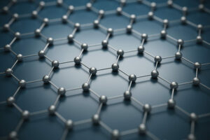
Graphene is a unique allotrope of carbon composed of a single atomic layer arranged in a two-dimensional honeycomb lattice. This structure imparts exceptional electronic properties, making graphene a subject of intense study in materials science and condensed matter physics. One of its most notable features is its classification as a zero band gap semiconductor, a property that distinguishes it from conventional semiconductors and underpins its potential in various technological applications.
Fundamentals of Band Theory in Semiconductors
To understand why graphene is considered a zero band gap semiconductor, it is essential to revisit the basics of band theory. In typical semiconductors, the electronic structure consists of two main energy bands: the valence band, which is fully occupied by electrons, and the conduction band, where electrons can move freely and contribute to electrical conductivity. The energy difference between these bands, known as the band gap, is a critical parameter that governs the electrical and optical behavior of the material.
- Valence Band:
The highest range of electron energies where electrons are normally present at absolute zero temperature. - Conduction Band:
The energy band above the valence band where electrons are free to move and conduct electricity. - Band Gap:
The energy interval between the valence and conduction bands; its size determines the semiconductor’s ability to control electron flow.
Materials like silicon and gallium arsenide have a well-defined band gap that allows for precise control of electrical conductivity through doping and other modifications.
Electronic Structure of Graphene
Graphene’s electronic properties diverge from classical semiconductors due to its distinctive band structure. The carbon atoms’ p-orbitals overlap to form π (bonding) and π* (anti-bonding) bands. At specific points in the reciprocal space, known as the K points within the first Brillouin zone, the conduction and valence bands converge, resulting in the absence of a band gap.
- Dirac Points:
Locations in momentum space where the conduction and valence bands meet, leading to zero band gap. - Linear Dispersion Relation:
Near the Dirac points, the energy of electrons varies linearly with momentum, resembling relativistic particles.
This unique band structure enables electrons in graphene to behave as massless Dirac fermions, facilitating extraordinary electron mobility and conductivity.
Implications of Zero Band Gap in Graphene
The zero band gap characteristic of graphene has profound effects on its electronic and optical properties:
- Exceptional Carrier Mobility:
Graphene exhibits electron mobilities exceeding 200,000 cm²/Vs at room temperature, surpassing traditional semiconductors and enabling ultra-fast electronic devices. - Optical Transparency:
Unlike typical semiconductors that absorb specific light wavelengths, graphene absorbs only about 2.3% of visible light, making it nearly transparent and ideal for applications like transparent conductive films and photovoltaic cells.
Challenges and Strategies for Band Gap Engineering
While the zero band gap endows graphene with remarkable properties, it also limits its use in applications requiring an on/off switching behavior, such as digital logic circuits. Without a band gap, graphene cannot be fully switched off, posing a challenge for conventional semiconductor device architectures.
To overcome this, researchers have developed various methods to induce a band gap in graphene:
- Chemical Functionalization:
Introducing chemical groups to modify electronic properties and open a band gap. - Layer Stacking:
Arranging graphene layers laterally or vertically to alter band structure. - External Electric Fields:
Applying fields to manipulate electron distribution and create a tunable band gap.
These approaches aim to combine graphene’s superior conductivity with the controllability of traditional semiconductors.
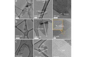
Graphene Synthesis Techniques
The production of graphene is a critical factor influencing its practical applications. Various synthesis methods have been developed, each with distinct advantages and limitations:
- Mechanical Exfoliation:
Peeling layers from graphite to obtain high-quality graphene, though limited in scalability. - Chemical Vapor Deposition (CVD):
Growing graphene on metal substrates, offering better scalability and uniformity. - Liquid-Phase Exfoliation:
Dispersing graphite in solvents to produce graphene flakes, useful for bulk production but with variable quality.
The choice of synthesis method affects graphene’s purity, layer uniformity, and integration potential in devices.
Mechanical and Biomedical Applications
Beyond its electronic and optical properties, graphene’s mechanical strength and flexibility open avenues for multifunctional devices. Its tensile strength surpasses that of steel, while maintaining remarkable flexibility, enabling the development of hybrid systems that integrate electrical, optical, and mechanical functionalities.
In the biomedical field, graphene’s biocompatibility combined with its electronic characteristics has led to promising applications such as biosensors and targeted drug delivery systems, highlighting its versatility across disciplines.
Why Graphene’s Zero Band Gap Matters
The zero band gap nature of graphene represents both a challenge and an opportunity in the advancement of materials science and technology. While it restricts graphene’s use in traditional semiconductor roles, it simultaneously offers unparalleled electronic and optical properties that could revolutionize high-speed electronics, optoelectronics, and flexible devices.
Ongoing research continues to explore ways to harness graphene’s strengths while mitigating its limitations, positioning it as a cornerstone material in the future landscape of advanced technologies.
FAQ
What is graphene?
Graphene is a single layer of carbon atoms arranged in a two-dimensional honeycomb lattice known for its exceptional electrical and mechanical properties.
Why is graphene considered a zero band gap semiconductor?
Graphene is classified as a zero band gap semiconductor because its conduction and valence bands meet at certain points in its electronic structure, allowing electrons to flow freely without a band gap.
What are the implications of graphene's zero band gap?
The zero band gap allows for exceptional electron mobility but limits graphene's use in applications requiring an on/off switch, such as digital logic circuits.


Leave a Reply