Short Answer
Definition of Quasi-Two-Dimensional Materials
Quasi-two-dimensional (quasi-2D) materials represent a unique class of substances that occupy the dimensional space between traditional two-dimensional (2D) materials and their bulk three-dimensional (3D) counterparts. Unlike strictly 2D materials, which are typically a single atomic layer or just a few layers thick, quasi-2D materials have thicknesses ranging from a few nanometers up to several tens of nanometers. This intermediate thickness imparts them with hybrid properties that blend characteristics of both 2D and bulk materials.
- Dimensional Classification:
Materials are categorized by their spatial dimensions: zero-dimensional (0D), one-dimensional (1D), two-dimensional (2D), and three-dimensional (3D). Quasi-2D materials bridge the gap between 2D and 3D. - Thickness Range:
Typically, quasi-2D materials have thicknesses between approximately 2 and 10 nanometers, though this can extend up to several tens of nanometers depending on the material and context. - Examples:
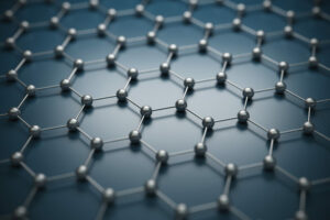
Common 2D materials include graphene and transition metal dichalcogenides (TMDs) such as molybdenum disulfide (MoS2), while their few-layer or thin-film forms often fall into the quasi-2D category.
Fundamental Mechanisms Behind Quasi-2D Behavior
The transition from bulk to quasi-2D materials is governed by quantum confinement and surface effects that become significant at nanoscale thicknesses. As the material’s thickness decreases, electrons experience spatial confinement, leading to discrete energy levels rather than continuous bands typical of bulk materials. This quantum confinement alters electrical, optical, and mechanical properties dramatically.
- Quantum Confinement:
When thickness approaches the nanoscale (around 10 nm or less), electron motion is restricted, resulting in quantized energy states that modify conductivity and optical absorption. - Surface and Edge Effects:
Reduced thickness increases the influence of surface atoms, defects, and edge states, which can dominate mechanical strength and chemical reactivity. - Interlayer Interactions:
Van der Waals forces and stacking orientation between layers affect the overall behavior, especially in layered materials like TMDs.
Mechanical Properties in the Quasi-2D Regime
Mechanical characteristics of materials undergo significant changes as they transition into the quasi-2D thickness range. Unlike bulk materials, where internal crystal defects primarily dictate strength and toughness, quasi-2D materials are more influenced by surface phenomena and atomic-scale imperfections.
- Enhanced Strength:
Studies show that few-layer TMDs can exhibit mechanical strengths exceeding their bulk forms due to reduced dislocation mobility and stronger atomic bonding. - Elasticity and Strain Limits:
Quasi-2D materials often demonstrate remarkable elasticity and can sustain higher strain before failure, attributed to their thinness and interlayer coupling. - Thickness-Dependent Stiffness:
The interplay between van der Waals forces and layer orientation contributes to increased stiffness within the 2-10 nm thickness range.
Electronic and Optical Property Modulations
The electronic band structure and optical responses of materials are highly sensitive to thickness variations in the quasi-2D domain. This sensitivity enables tuning of material properties for specific technological applications.
- Band Gap Evolution:
For example, bulk MoS2 exhibits an indirect band gap, whereas its monolayer form has a direct band gap, enhancing its interaction with light and suitability for optoelectronics. - Photoluminescence Enhancement:
Few-layer TMDs show increased photoluminescence intensity compared to bulk, making them promising candidates for photonic devices. - Light Absorption and Transmission:
Reduced thickness leads to unique optical phenomena such as increased light transmission and modified emissivity.
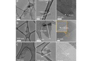
Fabrication Techniques for Quasi-2D Materials
Producing quasi-2D materials with precise control over thickness and properties requires advanced fabrication methods. These techniques enable researchers to tailor materials for desired functionalities.
- Mechanical Exfoliation:
Peeling thin layers from bulk crystals to obtain few-layer films. - Chemical Vapor Deposition (CVD):
Growing thin films layer-by-layer on substrates with controlled thickness. - Liquid-Phase Exfoliation:
Using solvents and sonication to separate layers into thin flakes.
Determining the Thickness Threshold for Quasi-2D Classification
The precise boundary between bulk, quasi-2D, and strictly 2D materials is not fixed and depends on intrinsic material properties and external conditions. Generally, when thickness falls below approximately 10 nanometers, quantum and surface effects become dominant, marking the onset of quasi-2D behavior. However, this threshold can vary based on the material’s crystal structure, interlayer bonding, and environmental factors.
Common Misconceptions About Quasi-2D Materials
Quasi-2D materials are simply thinner versions of bulk materials.
They exhibit fundamentally different properties due to quantum confinement and surface effects, not just reduced size.
All properties scale linearly with thickness.
Many properties change nonlinearly, with abrupt transitions occurring at nanoscale thicknesses.
Quasi-2D materials behave identically to monolayer 2D materials.
Quasi-2D materials often retain some bulk-like characteristics while also showing unique intermediate behaviors.
Significance of Quasi-2D Materials in Science and Technology
The study of quasi-2D materials is crucial for advancing material science and enabling next-generation technologies. Their tunable mechanical, electronic, and optical properties open pathways for innovations in flexible electronics, photodetectors, transistors, and photonic devices. Understanding the dimensional crossover from bulk to quasi-2D enriches fundamental physics and supports the design of materials with customized functionalities for diverse applications.
Summary
Quasi-two-dimensional materials occupy a fascinating niche between bulk and strictly two-dimensional substances, characterized by thickness-dependent transformations in their physical properties. Quantum confinement, surface effects, and interlayer interactions collectively define their unique behaviors. Advances in fabrication techniques allow precise control over these materials, facilitating their integration into cutting-edge technologies. As research progresses, the nuanced understanding of quasi-2D materials will continue to expand, driving innovation across multiple scientific and engineering fields.
FAQ
What is the thickness range for quasi-2D materials?
Quasi-2D materials typically have thicknesses from 2 to 10 nanometers, bridging the gap between single-layer 2D materials and bulk materials.
How does thickness reduction affect electrical properties?
Reducing thickness leads to quantum confinement effects, which can change the bandgap from indirect to direct and influence conductivity and optical absorption.
Why are quasi-2D materials important in technology?
Their unique mechanical, electronic, and optical properties enable applications in flexible electronics, photodetectors, and other advanced devices.
What fabrication techniques are used for quasi-2D materials?
Mechanical exfoliation, chemical vapor deposition, and liquid-phase exfoliation are common methods to create thin films with controlled thickness.
How do mechanical properties change in quasi-2D materials?
Mechanical strength and elasticity often increase due to reduced dislocation movement and dominant surface and edge effects.


Leave a Reply