Short Answer
Definition of Van der Waals Semiconductors
Van der Waals semiconductors are a distinctive category of materials characterized by their two-dimensional (2D) atomic layer structures and semiconductor behavior. Unlike conventional semiconductors that depend primarily on strong covalent bonds, these materials maintain their layered architecture through relatively weak van der Waals forces-interactions arising from transient dipole moments between electrically neutral atoms. This unique bonding mechanism becomes especially significant in ultra-thin, atomically layered materials.
- Van der Waals Forces:
Weak intermolecular attractions that hold layers together without strong chemical bonds. - 2D Atomic Layers:
Materials composed of single or few atomic layers, enabling novel electronic and optical properties.
Common Types and Composition
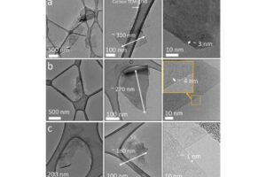
Van der Waals semiconductors predominantly include transition metal dichalcogenides (TMDs) such as molybdenum disulfide (MoS2), tungsten disulfide (WS2), and tungsten diselenide (WSe2). Other notable 2D materials in this class are black phosphorus and graphene. These substances can be exfoliated down to monolayers, allowing precise control over their physical and chemical characteristics.
Electronic Band Structure and Dimensionality Effects
The electronic properties of van der Waals semiconductors are profoundly influenced by their reduced dimensionality. While bulk TMDs typically exhibit indirect bandgaps, thinning these materials to a single atomic layer often results in a direct bandgap. This transition is crucial for optoelectronic applications, as direct bandgap materials efficiently absorb and emit light, unlike their bulk counterparts.
- Indirect vs. Direct Bandgap:
Bulk materials have indirect bandgaps limiting light emission, whereas monolayer forms possess direct bandgaps enhancing photonic performance. - Impact on Electron Transport:
The band structure influences how electrons move, affecting device efficiency.
Optoelectronic Applications
The emergence of a direct bandgap in monolayer van der Waals semiconductors enables their use in light-emitting diodes (LEDs), photodetectors, and other photonic devices. Unlike traditional silicon, which lacks efficient light emission at room temperature, these materials can operate effectively under ambient conditions, paving the way for compact, integrated optoelectronic systems.
Defect Engineering and Material Tuning
Manipulating defects within van der Waals semiconductors offers a powerful approach to tailor their electronic and optical properties. Controlled introduction or mitigation of imperfections can enhance light absorption, photon emission, and carrier mobility. Layer composition strategies further enable bandgap modulation, allowing customized functionalities for specific applications.
Mechanical Properties and Flexibility
Due to their weak interlayer bonding, van der Waals semiconductors exhibit remarkable mechanical flexibility and resilience. This combination of electrical performance and mechanical robustness supports the development of flexible electronics capable of enduring significant mechanical deformation, which is vital for wearable devices and portable technologies.
Van der Waals Heterostructures
Stacking different 2D van der Waals materials creates heterostructures with novel quantum phenomena such as tunneling and exciton formation. These layered assemblies hold promise for next-generation electronic components, including advanced transistors, integrated circuits, and quantum computing elements, potentially revolutionizing computational efficiency and device miniaturization.
Fundamental Physics and Research Frontiers
Beyond practical applications, van der Waals semiconductors serve as a platform to explore complex quantum mechanical effects in low-dimensional systems. Investigations into phenomena like locality, coherence, and frustrated magnetism challenge traditional condensed matter theories and deepen our understanding of electronic behavior at the atomic scale.
Challenges in Large-Scale Production
Despite their promising properties, scaling van der Waals semiconductors for industrial use remains challenging. Techniques such as chemical vapor deposition (CVD) and liquid-phase exfoliation have made progress in producing single-layer materials, but achieving uniformity and reproducibility on a commercial scale requires further technological advancements.
Significance and Future Outlook
Van der Waals semiconductors represent a transformative class of materials with unique structural, electronic, and mechanical attributes. Their ability to combine flexibility with superior optoelectronic performance positions them at the forefront of next-generation device innovation. Continued research and development in this field are expected to yield breakthroughs that could redefine semiconductor technology and its applications across electronics, photonics, and quantum computing.
FAQ
What is a van der Waals semiconductor?
A van der Waals semiconductor is a material composed of stacked two-dimensional atomic layers held together by weak van der Waals forces, exhibiting semiconductor properties.
How do van der Waals forces influence these semiconductors?
Van der Waals forces enable weak interlayer coupling, allowing for exfoliation to atomic thickness and providing unique mechanical flexibility and tunable electronic properties.
Why are van der Waals semiconductors important for flexible electronics?
Their mechanical robustness and flexibility under mechanical stress make them ideal for wearable and portable electronic devices.
What are the primary materials used in van der Waals semiconductors?
Transition metal dichalcogenides such as MoS2, WS2, WSe2, along with black phosphorus and graphene.
What challenges limit the large-scale use of van der Waals semiconductors?
Challenges include achieving reproducible, uniform large-area synthesis and controlling defects to optimize electronic properties.


Leave a Reply