
Short Answer
Understanding Two-Dimensional Materials
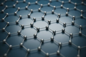
Two-dimensional (2D) materials are substances consisting of a single or a few atomic layers, exhibiting unique properties distinct from their bulk, three-dimensional counterparts. These atomically thin materials have garnered significant attention in recent years due to their exceptional electrical, mechanical, and thermal characteristics, which open new avenues for technological advancements.
- Atomic Thickness:
2D materials are typically only one or a few atoms thick, providing a flat, sheet-like structure. - Surface-Dominated Properties:
Unlike bulk materials, 2D materials emphasize surface interactions, where quantum effects become prominent. - Examples:
Graphene, transition metal dichalcogenides (TMDs), black phosphorus, and hexagonal boron nitride are notable 2D materials with diverse functionalities.
Significance and Advantages of 2D Materials
The fascination with 2D materials stems from their extraordinary capabilities that surpass traditional materials in several domains. Their ultra-thin nature allows for enhanced electrical conductivity, superior mechanical strength, and efficient thermal management. For instance, graphene is celebrated for its unparalleled conductivity and robustness, making it a benchmark in the field.
Moreover, the predominance of surface properties in 2D materials facilitates direct interaction with external stimuli, enabling applications that leverage quantum mechanical phenomena. This unique interaction landscape allows engineers to design devices with functionalities unattainable in conventional three-dimensional materials.
Varieties and Unique Properties of 2D Materials
Beyond graphene, the family of 2D materials includes several other compounds, each offering distinct advantages:
- Transition Metal Dichalcogenides (TMDs):
These materials possess tunable band gaps, making them ideal for optoelectronic applications such as photodetectors and light-emitting devices. - Black Phosphorus:
Known for its anisotropic electrical properties and adjustable band gap, it is promising for flexible electronics. - Hexagonal Boron Nitride (h-BN):
Often used as an insulating layer due to its excellent thermal and chemical stability.
Layered Architectures and Heterostructures
The structural design of 2D materials enables the creation of heterostructures-stacks of different 2D layers assembled vertically. This approach allows the combination of diverse material properties to produce synergistic effects, enhancing device performance beyond individual components.
Such heterostructures can be likened to culinary layering, where each ingredient contributes a unique flavor to the final dish. In engineering terms, stacking 2D materials can optimize electronic transfer, improve energy conversion efficiency, and enable novel functionalities in sensors, transistors, and energy storage devices.
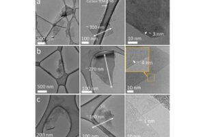
Synthesis and Scalability of 2D Materials
For practical applications, scalable production methods are essential. Techniques such as chemical vapor deposition (CVD) and liquid-phase exfoliation have been developed to fabricate large-area 2D materials while preserving their structural integrity.
- Chemical Vapor Deposition (CVD):
A process where gaseous precursors react on a substrate to form high-quality 2D films suitable for electronic devices. - Liquid Exfoliation:
Involves separating layers from bulk materials in a liquid medium, enabling mass production of 2D flakes.
These scalable methods ensure that 2D materials can transition from laboratory research to industrial applications, addressing the growing demand for miniaturized and high-performance technologies.
Challenges in Integrating 2D Materials
Despite their promising attributes, incorporating 2D materials into existing technologies presents several obstacles. One major challenge is achieving seamless integration between 2D layers and conventional three-dimensional systems, which requires careful engineering to maintain interface quality and device reliability.
Additionally, the delicate nature of 2D materials makes them vulnerable to environmental degradation, such as oxidation and moisture exposure. This fragility necessitates the development of protective strategies, including encapsulation and composite formation, to enhance durability and operational lifespan.
Environmental and Sustainability Considerations
The production and utilization of 2D materials also intersect with sustainability goals. Many synthesis methods employ non-toxic precursors and offer potential for recycling, aligning with eco-friendly manufacturing practices.
By integrating nanoscale innovation with environmental responsibility, the advancement of 2D materials can contribute to sustainable technological progress, minimizing ecological impact while maximizing performance.
Applications and Future Prospects
The exploration of 2D materials is revolutionizing multiple sectors, including electronics, photonics, catalysis, and energy storage. Their unique properties enable the development of ultra-sensitive sensors, flexible electronic devices, efficient energy converters, and novel photonic components.
As research continues, the engineering community is poised to unlock further potential, overcoming current limitations and expanding the horizons of material science. The journey into the two-dimensional realm represents a transformative shift, promising innovations that could redefine the technological landscape.
Common Misconceptions About 2D Materials
2D materials are just thinner versions of bulk materials.
Their properties differ fundamentally due to quantum confinement and surface effects, leading to unique behaviors not observed in bulk forms.
2D materials are too fragile for practical use.
While delicate, advances in encapsulation and composite technologies enhance their robustness for real-world applications.
Conclusion: The Transformative Impact of 2D Materials
The study and application of two-dimensional materials signify more than a scientific trend; they embody a paradigm shift in material engineering. By harnessing the distinctive properties of atomically thin layers, engineers are pioneering new technologies that promise to reshape industries and improve everyday life. As the field evolves, continued innovation and interdisciplinary collaboration will be key to fully realizing the vast potential embedded within these flat, yet profoundly powerful, materials.
FAQ
What are the advantages of 2D materials?
2D materials offer enhanced electrical conductivity, superior mechanical strength, and efficient thermal management.
How are 2D materials synthesized?
Common methods include chemical vapor deposition (CVD) and liquid-phase exfoliation.


Leave a Reply