Boron, traditionally recognized for its role in agriculture and chemistry, has begun to garner attention as a potential semiconductor material. Historically, semiconductors have relied heavily on elements like silicon and germanium, which have long been considered the staples of electronic devices. Amidst the landscape of evolving technologies, the prospect of utilizing boron as a semiconductor prompts a profound re-examination of conventional paradigms. This discussion aims to explore the intricate nature of boron while elucidating its theoretical and practical implications within the realm of semiconductor physics.
Firstly, understanding whether boron can be classified as a semiconductor necessitates addressing the fundamental characteristics that define semiconductors. Semiconductors, by definition, exhibit electrical conductivity between that of insulators and conductors, a behavior primarily attributed to their electron band structure. The valence band, comprised of electrons involved in bonding, functions alongside the conduction band, where free electrons facilitate conduction. The energy gap—the bandgap—between these two bands determines a material’s conductive properties. For a material to be deemed a semiconductor, it generally possesses a bandgap that can be bridged through thermal excitation or impurity doping.
Boron, depending on its allotrope, displays unique electronic properties. In crystalline form, it contributes to exceptional hardness and structural integrity, but its conductivity lacks the requisite attributes of traditional semiconductors. The diamond-like structure of boron allows for the formation of covalent bonds. This distinctive bonding configuration results in a complex band structure; boron has an indirect bandgap of approximately 0.4 eV, which is comparatively small. Intriguingly, this near-semiconductor property sparks curiosity regarding its potential applications in the semiconductor industry.
Several phenomena emerge when boron is doped into semiconductor matrices. When introduced into silicon, for example, boron acts as a p-type dopant. This means it can create ‘holes’ in the silicon lattice, facilitating the conduction process through the movement of positive charge carriers—essentially modifying the electrical properties of the silicon to enhance its suitability in various applications. The synergetic effects observed when integrating boron within well-established semiconductor platforms present a viable avenue for research, indicating that boron may serve as a key component in aforementioned p-n junctions.
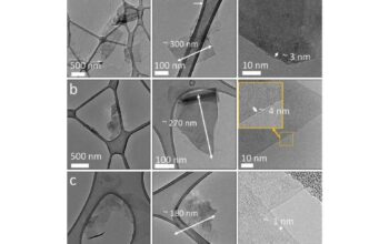
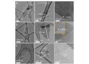
Having established an understanding of boron’s electronic behavior and potential for doping, it is imperative to delve into more innovative aspects of boron in semiconductor applications. Recent advancements in nanotechnology have elucidated that boron nanostructures, such as boron nanotubes and boron nitride, exhibit electrical characteristics that warrant consideration for future devices. These boron-based nanostructures boast remarkable thermal and chemical stability and possess unique electronic properties that could potentially rival conventional materials. Although the manipulation of these nanostructures requires advanced engineering techniques, their outstanding features are enticing for applications within electronic circuitry and photovoltaics.
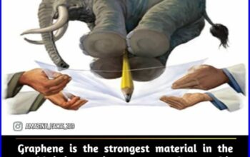
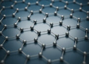
Moreover, the incorporation of boron into novel semiconductor technologies has far-reaching implications. The burgeoning field of two-dimensional materials, exemplified by graphene and transition metal dichalcogenides, is experiencing an influx of research into the integration of boron. By leveraging boron-doped configurations within these materials, researchers have explored enhanced charge carrier mobility and novel photonic properties, which may lead to the development of next-generation optoelectronic devices. Such advancements promise to facilitate faster data processing speeds and lower energy consumption, critical factors in our evolving technological landscape.
Despite the promising prospects of boron as a semiconductor, challenges remain. For one, synthesizing high-purity boron and achieving refined doping techniques necessitates further exploration. Investigating the stability and scalability of boron-based structures is paramount to determining their feasibility for industrial applications. Additionally, the integration of boron into existing semiconductor manufacturing processes could require substantial innovation in production methods. The ecosystem surrounding semiconductor fabrication is intricate, and any new material must meet stringent performance benchmarks to facilitate its adoption.
Examining the eco-conscious perspective of semiconductor production highlights another dimension in which boron could facilitate a shift in practices. Boron is relatively abundant in nature, making it an appealing alternative to more scarce materials utilized in traditional semiconductors. Its incorporation could pave the way for more sustainable electronic components, thus aligning with global efforts to reduce the environmental impact of technology. This critical examination of resource utilization further accentuates the need to foster interdisciplinary approaches within material science, electrical engineering, and environmental studies.
In conclusion, while boron currently does not meet the conventional parameters of a semiconductor, its unique properties, especially as a dopant and within novel nanostructures, herald an intriguing vista for future research. The integration of boron into semiconductor technologies presents a confluence of opportunities that invite researchers and engineers to innovate. As the demand for more efficient and sustainable electronic devices escalates, the exploration of boron’s potential within semiconductor physics stimulates both curiosity and hope within the academic community. The journey of boron from a merely pedagogical element to a potential cornerstone of future semiconductor developments exemplifies the constant evolution of materials science, beckoning a redefined era in technology that encourages scholarly inquiry and creative thought.