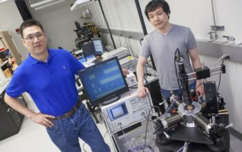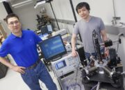
Boron nitride, a compound known primarily for its thermal and chemical stability, has emerged as a fascinating subject for researchers investigating the quantum phenomena of electron tunneling. Recent breakthroughs illustrate a pivotal shift in our understanding of how electrons interact with materials at the nanoscale. This discovery not only broadens the horizon of material science but also delineates a new chapter in the development of advanced electronic devices, promising remarkable applications in various fields including quantum computing and optoelectronics.
To elucidate the significance of electron tunneling in boron nitride, it is essential to grasp the underlying principles of quantum mechanics that govern this behavior. Electron tunneling occurs when electrons traverse a potential barrier, a phenomenon that distinguishes itself from classical physics predictions. At the heart of this transformative process is the concept of wave-particle duality, permitting electrons to exhibit both particle-like and wave-like characteristics. Consequently, the penetration of electrons through barriers that would typically impede their flow is not merely a theoretical curiosity but a testament to the intricacies of quantum mechanics.
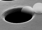
Traditionally, materials characterized as insulators, such as boron nitride, were not expected to facilitate significant electron movement. However, experimental observations reveal a striking proficiency in this compound’s ability to allow electrons to tunnel with remarkable ease. This contradicts conventional expectations and calls into question existing paradigms surrounding material conductivity. The superior properties exhibited by boron nitride can be primarily attributed to its unique crystalline structure and the presence of sp2 and sp3 hybridization, which bestow it with distinctive electronic characteristics.
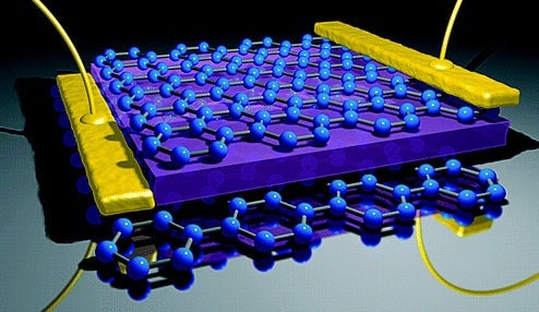
The crystal lattice of boron nitride manifests in various allotropes, the most notable being hexagonal boron nitride (h-BN) and cubic boron nitride (c-BN). The hexagonal form, often referred to as “white graphene,” bears analogies to graphene due to its two-dimensional nature and strong covalent bonds. Such structural attributes lead to an intriguing juxtaposition of insulating properties alongside the potential for facilitating quantum transport phenomena. Conversely, cubic boron nitride exhibits exceptional hardness and thermal stability, finding its niche primarily in industrial applications. However, it is the hexagonal variant that has captured the attention of scientists delving into quantum electron transport.
The tunability of electronic properties in boron nitride is particularly captivating. By manipulating defects within the lattice structure, researchers have demonstrated the ability to introduce localized states that can trap electrons. These traps can serve as gateways for tunneling events, enhancing the overall tunneling probability. This tunability not only elucidates the fundamental mechanics of tunneling in boron nitride but also signifies a major leap toward engineered materials designed for specific applications. The capacity to control electron pathways opens new avenues for innovation, particularly in the realm of quantum computing, where efficient electron transfer is paramount.
Moreover, the implications of efficient tunneling in boron nitride extend into the arena of optoelectronics. Devices that dynamically manipulate light and electrons often rely on precise electron transport mechanisms. The advent of boron nitride as an enabling material for tunneling provides a viable substrate for the development of advanced photonic devices. Such materials could catalyze improvements in light-emitting diodes (LEDs), photodetectors, and even solar cells, harnessing the unique tunneling characteristics to optimize performance and energy efficiency.
As researchers delve deeper into the symbiotic relationship between electron tunneling and the properties of boron nitride, numerous pathways for future exploration arise. Notably, the integration of boron nitride with other two-dimensional materials such as transition metal dichalcogenides could yield heterostructures exhibiting exotic electronic and optoelectronic properties. The formation of van der Waals heterostructures not only capitalizes on the unique attributes of boron nitride but also offers an engaging platform to probe novel physical phenomena, including superconductivity and magnetic effects at the nanoscale.
The potential applications of boron nitride are manifold and reach beyond conventional electronics. In the realm of nanotechnology, its inherent robustness and biocompatibility position it favorably for use in biomedical devices. The material’s thermal stability, alongside its ability to facilitate electron tunneling, opens avenues for employing boron nitride in sensors and drug delivery systems. This interdisciplinary approach highlights the importance of fundamental research in bridging gaps between physics, materials science, and engineering.
In conclusion, the advent of boron nitride as a material that facilitates electron tunneling with ease marks a significant departure from traditional views on insulating materials. This discovery not only challenges established paradigms but also paves the way for transformative applications across technology sectors. The intricate interplay between quantum mechanics and material properties imbues boron nitride with a unique character that beckons further exploration. As research unfolds, the allure of boron nitride in the ongoing quest to harness quantum phenomena promises not only to pique curiosity but also to redefine our technological landscape.