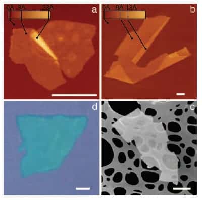
In the realm of condensed matter physics, the emergence of two-dimensional (2D) atomic crystals has catalyzed a paradigm shift in our understanding of material properties. These materials—such as graphene, molybdenum disulfide (MoS2), and hexagonal boron nitride (h-BN)—exemplify a burgeoning class of substances characterized by their extraordinary physical and chemical properties. The transition from three-dimensional (3D) materials to a strictly 2D geometry unveils unique interactions among atoms, electrons, and phonons, thus laying the groundwork for a fascinating field of study that has captivated the scientific community.
The allure of 2D atomic crystals transcends their structural simplicity. The possibility of tuning these materials at the atomic level beckons researchers to explore their potential applications in next-generation electronic, photonic, and even quantum devices. For instance, the exceptional electrical conductivity of graphene has ignited enthusiasm around its application in high-speed transistors and transparent conductive coatings. Analogously, the semiconducting nature of MoS2 makes it a candidate for use in photodetectors and flexible electronic devices. Such profound implications are rooted in the unique electronic band structures that arise due to the constraints imposed by a two-dimensional lattice configuration.
Electronic band structure is fundamentally altered when one transitions from bulk to 2D materials. In three-dimensional solids, the electronic states are typically influenced by various interlayer interactions. In stark contrast, the reduced dimensionality in 2D crystals results in a distinct bandgap that can be modulated through external stimuli such as electrostatic gating or mechanical strain. This tunability presents an exquisite opportunity to engineer materials for specific functionalities, fostering innovative designs in nanoscale electronics.
Equally compelling is the manipulation of phonon modes in 2D materials. The phonon dispersion curves, which describe the vibrational modes of the lattice, exhibit a pronounced dependence on the dimensionality of the material. For instance, the absence of out-of-plane optical phonons in monolayer graphene significantly alters its thermal conductivity compared to its bulk counterpart. By understanding these phononic behaviors, researchers can devise strategies to engineer thermal management solutions or novel thermoelectric materials that can efficiently convert temperature differences into usable energy.
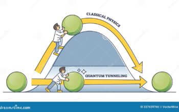
The study of 2D atomic crystals invites profound inquiry into the intriguing realm of quantum phenomena. Quantum tunneling and the emergence of quantum Hall effects have been empirically realized in these materials, further illuminating the intersection of theory and experimental validation. Notably, when doped with certain elements, these materials exhibit superconducting properties at relatively high temperatures. Such breakthroughs underscore the significance of 2D materials as a fertile ground for exploring exotic quantum states, which may pave the way towards more efficient quantum computing architectures.
Nonetheless, the intrinsic properties of 2D atomic crystals raise crucial considerations surrounding stability and scalability. The lack of bulk supporting substrates renders these materials susceptible to environmental degradation. Therefore, encapsulation techniques and protective coatings are paramount for maintaining the functionality of devices fabricated from 2D crystals. Furthermore, the synthesis of high-quality monolayers that can be reliably produced on a commercial scale remains a significant challenge, necessitating advancements in methodologies such as chemical vapor deposition (CVD) and liquid-phase exfoliation.
Moreover, the interlayer interactions in heterostructures formed from stacking various 2D materials can give rise to emergent behaviors that are not present in the individual layers alone. The formation of van der Waals heterostructures has opened avenues for constructing devices with multifunctional capabilities, merging distinct properties of the constituent materials. The superposition of different electronic or optical properties within a heterostructured stack could lead researchers towards novel applications that have yet to be conceptualized.
As 2D materials gain widespread interest, their applications extend beyond conventional electronics. Emerging research points towards practical trajectories in energy storage and conversion systems, particularly with respect to lithium-ion batteries and supercapacitors. The exceptionally high surface area of 2D materials facilitates the adsorption of ions, enhancing the efficiency of charge transfer processes. Investigating the interaction of 2D materials with biological systems has also unveiled potential prospects in the field of biomedicine, particularly in drug delivery and biosensing applications.
In conclusion, the emergence of 2D atomic crystals is a testimony to the spirit of scientific inquiry and innovation. This domain not only challenges existing paradigms within condensed matter physics but also dramatically reshapes the landscape for future technological advancements. The harmonious interplay between fundamental physics and applied research in 2D materials offers a unique vantage point, unveiling the underlying principles that govern their unique properties. As researchers continue to unveil the mysteries of flatland physics, the potential ramifications of these discoveries are limitless, casting a bright trajectory for both fundamental science and revolutionary applications.


