The quest for the thinnest material, both synthesized and naturally occurring, has captivated researchers and scientists alike, inciting a multitude of inquiries into the fundamental properties of matter. As the field of materials science evolves, the nomenclature regarding material thickness has taken on new dimensions, necessitating a detailed exploration of what constitutes the “thinnest” material. At the forefront of this discussion is graphene, a single layer of carbon atoms arranged in a two-dimensional lattice, often heralded as the world’s thinnest material. Its remarkable characteristics have raised profound questions about the very nature of materials and their potential applications.
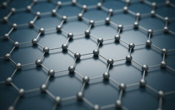
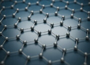
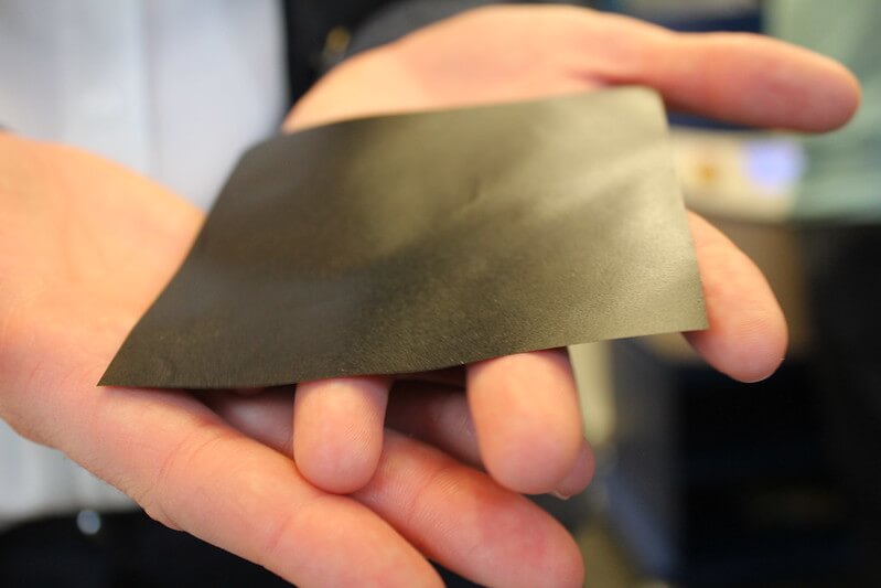
Graphene epitomizes the allure of two-dimensional materials. Comprising a mere one atom in thickness, this monolayer arrangement has been synthesized through various methods including chemical vapor deposition and mechanical exfoliation. Researchers have marveled at its extraordinary electrical conductivity, mechanical strength, and thermal properties. These attributes not only signify its potential utility in a diverse array of applications, including electronics, nanotechnology, and biomedical fields, but also underscore a deeper philosophical contemplation regarding dimensionality and materiality.
To fully appreciate the significance of graphene, one must delve into the underlying science that informs its properties. The honeycomb structure of graphene endows it with a unique band structure that facilitates the swift movement of electrons, thus establishing its status as one of the best conductors of electricity known to date. This phenomenon is attributed to its pi-bonding electrons, which are delocalized over the entire lattice, allowing for exceptional mobility without significant energy loss. Such characteristics make graphene a prime candidate for next-generation circuitry, potentially leading to more efficient electronic devices compared to those currently in use.
Moreover, graphene’s tensile strength is astonishing, being approximately 200 times stronger than steel. This extraordinary resilience stems from the covalent bonds that form between the carbon atoms within its structure, which confer both robustness and an ability to withstand significant deformation. The exploration of graphene’s strength potency has prompted investigations into its use in composite materials, enhancing the mechanical properties of various products ranging from sporting goods to construction materials.
However, the fascination with the thinnest materials does not begin and end with graphene. Beyond its monolayer structure, researchers have turned their attention to other two-dimensional materials such as transition metal dichalcogenides (TMDs). TMDs, including materials like molybdenum disulfide (MoS2), exhibit remarkable electronic and optical properties akin to those of graphene. In particular, the semiconducting nature of TMDs opens avenues for their incorporation into electronic devices where a bandgap is desirable—a feature absent in graphene. The exploration of these materials has broadened the definition of “thin”, inviting new opportunities in material design and application.
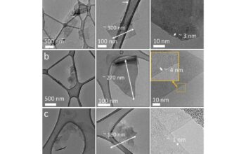
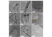
Transitioning from synthetic to naturally occurring two-dimensional materials reveals yet another dimension to the discourse surrounding thinness. Mica, a naturally occurring mineral, exhibits layers that can be easily separated to generate ultra-thin sheets. Such separations yield phyllosilicate layers that can be mere nanometers in thickness. While mica does not rival the atomic scale of graphene, its remarkable cleavage properties render it one of the thinnest natural materials accessible to researchers. The study of mica layers contributes to an understanding of layered materials and their potential utility in various applications, from electronics to optics.
Another intriguing candidate for the title of thinnest material is a class of materials known as MXenes, which are derived from the selective etching of layered transition metal carbides. Similar to graphene, MXenes are conductive and have generated excitement for their potential in energy storage applications, particularly in supercapacitors and batteries. Their composition and structure allow for tunable properties which can be manipulated for specific functionalities, showcasing the ongoing evolution in our understanding of two-dimensional materials.
As we continue to probe the boundaries of materials science, the emphasis on thinness raises significant implications for a multitude of disciplines. From electronic engineering to biomedical applications, the versatility and potential of materials at the atomic or molecular level challenge conventional paradigms. The intrinsic properties of these materials unveil a new frontier where quantum mechanical principles manifest on macroscopic scales, and the measurement of thinness transcends mere dimensionality to explore the associational intricacies of interactions amongst quantum states.
In conclusion, the pursuit of the thinnest material illuminates not just the fascination inherent in material science but also a profound desire to understand the fundamental nature of matter. Graphene, transition metal dichalcogenides, and MXenes exemplify the diverse characteristics and applications achievable through materials at the atomic scale, laying the groundwork for innovations that span multiple fields. The challenges posed by these diminutive structures are not merely technical; they beckon a philosophical examination of the relationship between dimensionality, utility, and the broad expanse of possibilities that lie at our fingertips. As research uncovers ever-thinner materials, the broader implications for technology, sustainability, and our comprehension of physical laws continue to unfold, further enriching the tapestry of scientific knowledge.