Two-dimensional (2D) materials have captivated the scientific community with their unique properties and potential applications across various fields. Graphene, the most notable of these materials, exemplifies the extraordinary promise of 2D structures. However, while the excitement surrounding 2D materials is palpable, they inherently embody a range of advantages and disadvantages that merit thorough examination. This discourse explores the multifaceted realm of 2D materials, raising the question: Do the substantial advantages of 2D materials eclipse their notable limitations, or is there an equilibrium that researchers must navigate?
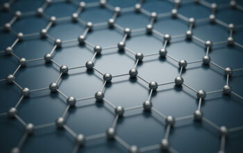
At the crux of the allure surrounding 2D materials is their atomic thinness, which imparts remarkable mechanical, electrical, and thermal properties. The quintessential example, graphene, composed of a singular layer of carbon atoms, exhibits exceptional electrical conductivity and flexibility. This property renders it an unparalleled candidate for applications in nanoelectronics, where miniaturization is paramount. The high surface area-to-volume ratio of 2D materials further accentuates their utility in catalysis and energy storage, providing efficient charge transfer and rapid reaction rates.
Moreover, the quantum confinement effects that arise in 2D materials lead to fascinating optical characteristics. For instance, transition metal dichalcogenides (TMDs), such as MoS2, have emerged as novel semiconducting materials with tunable bandgaps. This property allows for their strategic use in photonic applications, including light-emitting devices and photodetectors, which could revolutionize modern technologies. Indeed, these characteristics prompt a ponderous reflection: as we advance towards the paradigm of ultra-thin electronics, how do we ensure that the promises of 2D materials are met without succumbing to their inherent challenges?
However, while the advantages of 2D materials are compelling, it is imperative to address the latent drawbacks that accompany their utilization. One of the most significant challenges lies in the scalability of production methods. Many promising 2D materials are synthesized via techniques such as mechanical exfoliation or chemical vapor deposition, which may not be amenable to large-scale manufacturing. The costs and complexities associated with these methods can hinder the transition from laboratory settings to industrial applications. Can innovation in synthesis technologies bridge this gap, or will scalability remain a elusive goal?
Furthermore, the stability of 2D materials poses another conundrum. The environmental susceptibility of these materials can lead to degradation over time, impacting their performance in real-world applications. For example, graphene oxide is known to undergo reduction in ambient conditions, which can alter its electronic properties. The short-lived nature of certain 2D materials manifests a pressing question: how can we engineer enhanced durability without compromising the exceptional characteristics that have rendered these materials so compelling?
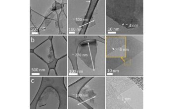
Another critical consideration is the interplay of defects within 2D materials. While defects can sometimes enhance a material’s properties, they often undermine the intrinsic advantages these materials offer. Consequently, understanding and controlling defect formation during fabrication becomes essential. Intriguingly, how do we manage the paradox that some defects can be beneficial while others are detrimental? This perplexing issue highlights the need for a nuanced approach to material design and engineering.
The integration of 2D materials into existing technologies further compounds these challenges. Traditional electronic devices are not designed to accommodate the unique characteristics of 2D materials, raising questions about compatibility and integration methods. The assembly of 2D materials with other materials—including bulk substrates—necessitates innovative strategies that consider the disparate properties at play. Can we surmount the difficulties posed by hybridization, or will the uniqueness of 2D materials remain confined to academic inquiry?
Despite these challenges, the horizon of 2D materials is not bleak. Innovative strategies in nanostructuring enable the tailoring of material properties to desired specifications, paving the way for advanced applications. Additionally, the advent of heterostructures—composite materials composed of two or more different 2D layers—opens a plethora of opportunities for compositions with customizable characteristics. Such advancements beckon further exploration into the boundaries of material science, nudging researchers to ponder: will heterostructures redefine the future landscape of integrated circuits?
Moreover, the potential of 2D materials in the realm of energy applications cannot be understated. Their superior charge carrier mobility and efficiency present promising prospects for advancements in batteries and supercapacitors. Research into using 2D materials for energy harvesting—such as photovoltaic cells—offers transformative possibilities in the quest for sustainable energy solutions. However, can these materials navigate the intricate balance of efficiency, longevity, and environmental compatibility in energy applications?
In conclusion, the discourse surrounding the merits and demerits of 2D materials reveals a complex narrative. While the benefits are significant and hold promising potential across various industries, the challenges inherent in their synthesis, stability, integration, and defect management cannot be overlooked. As researchers continue to push the boundaries of our understanding, the questions posed throughout this analysis remain crucial. Will the triumphs of 2D materials ultimately outweigh their challenges, or will their limitations necessitate a reevaluation of their immediate applicability? The journey into the realm of 2D materials is far from complete, beckoning continued inquiry and innovation.