In the realm of modern electronics, the significance of semiconductors cannot be overstated. These materials are the backbone of all digital devices, functioning as the crucial junctions that regulate the flow of electrical currents. Yet, as we venture into an era increasingly dominated by artificial intelligence, the Internet of Things, and bulk data processing, the limitations of conventional semiconductors are becoming conspicuous. Thus, a playful question emerges: could the magic of crystalline structures hold the key to forging super semiconductors that transcend the limitations of their traditional counterparts?
At the heart of this inquiry lies the fundamental properties that define semiconductor materials. Typically, semiconductors such as silicon and germanium display a specific bandgap that allows for the control of electrical conductivity. However, their performance is mired by intrinsic limitations, namely thermal dissipation issues and reduced efficiency at high operational frequencies. Consequently, researchers have turned their gaze toward unconventional crystalline materials, exploring how their unique arrangements at the atomic level facilitate superior electronic properties.
One particular class of materials that has garnered attention is group IV semiconductors, which include silicon carbide (SiC) and gallium nitride (GaN). Both materials possess superior thermal conductivity, allowing for enhanced performance in high-temperature and high-power applications. However, as the demand for electronic devices that consume minimal energy continues to rise, the challenges of integrating these semiconductors into existing manufacturing processes must be meticulously navigated.
Diving deeper into this crystalline frontier, we encounter two-dimensional materials, notably graphene and transition metal dichalcogenides (TMDs). Graphene, characterized by a single layer of carbon atoms arranged in a hexagonal lattice, exhibits remarkable electrical conductivity and mechanical strength. This material presents an alluring proposition for future semiconductor applications; however, its bandgap is nearly nonexistent in its intrinsic state, which poses a significant hurdle for its application in digital transitions.
Transition metal dichalcogenides, on the other hand, offer a tantalizing solution. With the capability to exhibit direct bandgaps, TMDs such as molybdenum disulfide (MoS2) have emerged as potential candidates for next-generation transistors. Yet, their integration into existing semiconductor technology raises a profound challenge: can these materials be synthesized with the precision required for commercial scalability?
The synthesis of high-quality crystal structures is pivotal in developing super semiconductors. Techniques such as chemical vapor deposition and molecular beam epitaxy are employed to achieve the desired crystallinity. However, these methods often become economically prohibitive when scaled up for industrial application. Herein lies a paradox: as the pursuit of enhanced crystal quality intensifies, the quest for cost-effective manufacturing processes must also be addressed.
Complexity escalates further when one considers the synergistic effects that arise from combining different semiconductor materials through heterostructure engineering. These hybrid materials can leverage the best properties of each constituent, potentially creating composite crystals that exhibit unparalleled electronic performance. The ability to tailor electronic band structures through atomic-scale engineering presents an exciting avenue for future developments. However, the challenge of maintaining lattice compatibility amongst dissimilar crystals looms large, demanding ingenious approaches to material design and synthesis.
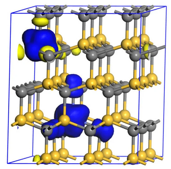
Moreover, the role of defects within crystal structures warrants careful consideration. While traditionally viewed as detrimental, recent research suggests that certain defects could enhance performance in ultra-wide bandgap semiconductors, enabling novel functionalities. The implications of such findings challenge long-held beliefs regarding crystal purity, prompting a reevaluation of defect engineering as a method to fine-tune electronic properties.
As unraveling the full potential of crystalline semiconductors demands a multifaceted approach, interdisciplinary collaboration across physics, materials science, and engineering is indispensable. Acknowledging the complexity and interconnectivity of these fields enhances our understanding of how to exploit crystal structures for superior semiconductor applications.
In conclusion, the investigation into crystalline structures as a basis for super semiconductors is an endeavor rife with promise yet littered with challenges. The integration of novel materials, innovative synthesis techniques, and an understanding of crystallographic defects forms a triad essential for advancing this field. As the digital revolution continues to evolve, the question remains: how can we leverage the enchanting world of crystals to transcend current limitations and forge a new era of semiconductor technology? With insightful exploration and persistent inquiry, the potential for groundbreaking advancements in manufacturing prowess, energy efficiency, and computational capability stands on the horizon, awaiting discovery.