The exploration of two-dimensional (2D) materials has captivated scientists across a multitude of disciplines, offering unique properties that are not only intriguing but also potentially transformative in various applications. To comprehend the significance of 2D materials, it is essential to delineate what constitutes quasi-2D materials and the threshold at which a piece of material transitions from bulk to quasi-2D. The thickness of a material plays a crucial role in determining its mechanical properties, electronic behaviors, and optical characteristics, fundamentally altering its performance and applicability.
At the heart of this inquiry lies the definition of quasi-2D materials. Traditionally, materials are classified based on their dimensionality: zero-dimensional (0D), one-dimensional (1D), two-dimensional (2D), and three-dimensional (3D). 2D materials, such as graphene and transition metal dichalcogenides (TMDs), exhibit properties that arise from their monolayer or few-layer thickness. In contrast, quasi-2D materials possess characteristics that bridge the gap between 2D and their bulk counterparts. This unique categorization typically pertains to materials with a thickness on the order of a few nanometers to several tens of nanometers. The fascination with this dimensional parameter emanates from the notable shift in material behavior as thickness diminishes.
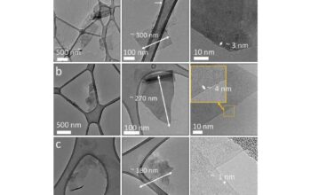
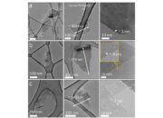
The quantum confinement effect is pivotal in understanding the transition to quasi-2D. In essence, as the thickness of a material approaches the nanoscale, the confinement of electrons becomes increasingly pronounced, leading to discrete energy levels rather than continuous bands as observed in bulk materials. This phenomenon is responsible for alterations in electrical conductivity, optical absorption, and mechanical responses. For many materials, when the thickness is reduced to approximately 10 nanometers or less, the quantum effects dominate, prompting a re-evaluation of their potential applications. Consequently, we must consider how such a transition affects various properties of materials when defining quasi-2D.
Mechanical properties provide a striking illustration of this transition. As the thickness of materials decreases, the conditions under which they are tested and employed change. For instance, in bulk materials, strength and toughness may be predominantly dictated by intrinsic crystal structures and defects. However, when assessing materials in the quasi-2D regime, surface effects, edge defects, and the presence of vacancies start to govern the mechanical integrity. Research indicates that as materials reach a few layers thick—particularly in TMDs—their mechanical strength can surpass that of their bulk counterparts, which is predicated on the reduced likelihood of dislocation movements and enhanced bond resilience.
Furthermore, a thickness range typically considered quasi-2D lies in the regime of 2 to 10 nanometers. Within this interval, materials typically exhibit extraordinary strain limits, remarkable elasticity, and increased stiffness. Not quickly apparent, however, is the underlying cause of these enhancements. The interplay between interlayer forces, van der Waals interactions, and the relative orientation of layers plays a pivotal role. This complexity enriches the investigation into quasi-2D materials, as researchers delve into not only thickness but also stacking configurations, layer orientation, and interlayer coupling mechanics that can drastically influence properties.
In addition to mechanical behaviors, the emergence of novel electronic properties warrants exploration. The band gap of semiconducting materials is particularly subject to modulation by the number of atomic layers. For instance, while bulk molybdenum disulfide (MoS2) is an indirect bandgap semiconductor, its monolayer counterpart assumes a direct bandgap characteristic. This transition significantly impacts light-matter interactions, determining applicability in optoelectronic devices. Thus, the thickness of materials becomes inherently linked to their utility in technological innovations, such as photodetectors, transistors, and flexible electronic devices.
Optical properties are yet another domain profoundly affected by the transition from bulk to quasi-2D. The thickness of a material influences how it interacts with light, including absorption and photoluminescence properties. As thickness decreases to the few-nanometer range, unique phenomena such as enhanced light transmission and altered emissivity can arise. Within this context, research has shown that few-layer TMDs exhibit higher photoluminescence intensities compared to their bulk analogs, sparking interest in their potential utility for advanced photonic applications.
Innovative fabrication techniques are required to precisely engineer materials at the quasi-2D level. Methods such as mechanical exfoliation, chemical vapor deposition, and liquid-phase exfoliation enable the creation of thin films with controlled thickness and predetermined properties. The ability to manipulate material thickness with such finesse opens new avenues for research, allowing scientists to tailor material characteristics to specific requirements.
Ultimately, the question of at what thickness a material transitions to quasi-2D is contingent upon a confluence of factors, including intrinsic material properties and external environmental influences. As investigations continue into this realm, the boundaries delineating 2D, quasi-2D, and bulk materials will become increasingly blurred. This ongoing exploration not only enriches our understanding of the fundamental physics governing material behavior but also paves the way for the discovery of novel applications spanning electronics, optics, and beyond.
In conclusion, defining quasi-2D materials necessitates careful consideration of a multi-faceted spectrum of properties, underpinned by thickness at the nanoscale. The profound implications of this dimensional transition reveal an intricate tapestry of relationships between mechanical, electronic, and optical characteristics. As the scientific community continues to probe the depths of these intriguing materials, the quest for understanding will undoubtedly yield further insights, broadening our horizons in material science and beyond.