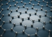
Graphene, an allotrope of carbon consisting of a single layer of atoms arranged in a two-dimensional honeycomb lattice, has garnered significant interest in the field of materials science and condensed matter physics. Its unique electronic properties render it a promising candidate for various applications, from electronic devices to advanced materials. One of the most intriguing characteristics of graphene is its classification as a zero band gap semiconductor. Understanding this property requires delving into the band structure of graphene, its implications, and the broader context within the realm of semiconductors.
To comprehend why graphene is designated as a zero band gap semiconductor, it is imperative to first review the fundamentals of band theory. In semiconductors, a band gap exists between the valence band, which is filled with electrons, and the conduction band, where electrons are free to move and contribute to conductivity. The size of this band gap is critical as it determines the electrical and optical properties of the material. Typical semiconductors, such as silicon or gallium arsenide, possess a distinctly quantifiable band gap that facilitates the control of electron flow; enabling the manipulation of electrical conductivity through doping and other chemical techniques.
However, graphene deviates from this classical description due to its peculiar electron band structure, which is derived from the overlapping of p-orbitals and the resultant formation of π and π* (anti-bonding) bands. At the corners of the first Brillouin zone, specifically at the K points, the conduction and valence bands meet; this feature leads to the conduction band and valence band merging, thereby eliminating the band gap. Thus, graphene stands out as a zero band gap semiconductor, where electron mobility is not only unimpeded but inherently spectacular due to the linear dispersion relation of the energy-momentum relationship.
The implications of graphene’s zero band gap are manifold. Firstly, this band structure bestows graphene with extraordinary electronic properties, including exceptionally high carrier mobility, which can exceed 200,000 cm²/Vs at room temperature. Such high mobility outstrips that of conventional semiconductors, making graphene an alluring material for high-frequency and high-speed electronic applications, such as transistors and sensors. The ability to conduct electricity with minimal resistance and rapid response times presents exciting opportunities for the development of next-generation electronic devices.
Moreover, the zero band gap characteristic of graphene influences its optical properties. In contrast to semiconductors with a finite band gap, which can become opaque to certain light wavelengths, graphene exhibits a unique transparency, absorbing only approximately 2.3% of visible light. This attribute renders it suitable for optical applications including transparent conductive coatings and photovoltaics. Interestingly, the optical response of graphene can be engineered by modifying its environment or by changing its thickness, a principle that paves the way for novel optoelectronic devices.
It’s worth noting that while the zero band gap property of graphene is advantageous, it also limits its ability to function as a traditional semiconductor in certain applications. For instance, without a band gap, graphene cannot be completely turned off, which poses challenges for its utilization in digital logic circuits where binary states are essential. As a result, researchers have sought to develop strategies for opening a band gap in graphene, such as chemical functionalization, lateral or vertical stacking of graphene layers, or applying external electric fields. These methods create hybrid materials that might harness the beneficial properties of graphene while introducing a controllable band gap.
Graphene’s zero band gap semiconductor property invites deeper contemplation regarding its potential in the future of electronics. The relentless pursuit of materials capable of revolutionizing energy storage and generation systems, as well as the ever-demanding field of computation, finds a rich terrain in graphene. Moreover, the synthesis of graphene—be it mechanical exfoliation, chemical vapor deposition, or liquid-phase exfoliation—remains an area of intense research. Each method presents its unique advantages and challenges concerning scalability, purity, and layer uniformity, all of which directly impact the feasibility of integrating graphene into practical applications.
Furthermore, the fascination surrounding graphene is underscored by its mechanical properties, such as tensile strength and flexibility. When juxtaposed with traditional semiconductors, these attributes facilitate the exploration of hybrid devices that merge electrical, optical, and mechanical functionalities. In biomedicine, for example, graphene’s biocompatibility, combined with its electronic properties, suggests promising applications in biosensors and drug delivery systems.
In conclusion, the reasons underpinning graphene’s classification as a zero band gap semiconductor are inherently linked to its unique electronic structure and the implications this structure entails for various technological applications. Graphene exhibits an intriguing paradox: while lacking a band gap restricts its functionality in standard semiconductor roles, it concurrently bestows remarkable electronic and optical characteristics that suggest transformative potential. The ongoing exploration of graphene not only addresses practical engineering challenges but also unveils deeper questions about the fundamental nature of materials and their interplay with technology. Whether grappling with its limitations or leveraging its strengths, graphene remains a pivotal focus in the quest for the next generation of advanced materials and devices.