Short Answer
Definition of Two-Dimensional Materials
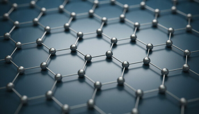
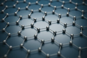
Two-dimensional (2D) materials are crystalline substances consisting of a single layer or a few atomic layers, exhibiting unique physical and chemical properties distinct from their bulk counterparts. These materials are characterized by their ultra-thin, planar structures, often just one atom thick, which grant them exceptional electrical, mechanical, and optical behaviors.
- Graphene:
A monolayer of carbon atoms arranged in a hexagonal lattice, renowned for its extraordinary conductivity and strength. - Transition Metal Dichalcogenides (TMDs):
Compounds like molybdenum disulfide (MoS2) and tungsten diselenide (WSe2) that exhibit semiconducting or metallic properties depending on their structure. - Phosphorene:
The monolayer form of black phosphorus, notable for its anisotropic electrical conductivity and tunable bandgap.
Historical Background and Emergence
The discovery of graphene in 2004 marked a pivotal moment in materials science, revealing the potential of atomically thin layers. Isolated through mechanical exfoliation, graphene’s remarkable electrical conductivity, mechanical robustness, and thermal properties sparked widespread research interest. This breakthrough catalyzed the search for other 2D materials, expanding the field beyond carbon-based structures to include a diverse array of layered compounds.
Varieties and Characteristics of 2D Materials
The family of 2D materials extends well beyond graphene, encompassing a broad spectrum of substances with distinct properties:
- Transition Metal Dichalcogenides (TMDs):
These materials, such as MoS2 and TiS2, possess layered structures that can be tuned to exhibit semiconducting or metallic behavior. Their band structures are highly sensitive to the number of layers and external stimuli, enabling versatile electronic applications. - Phosphorene:
Derived from black phosphorus, phosphorene displays direction-dependent electrical conductivity and a bandgap that can be adjusted, making it suitable for photodetectors and transistor technologies. - Other Emerging 2D Materials:
Materials like graphyne and 2D ferromagnets introduce metalloid and magnetic properties, respectively, broadening the functional landscape of 2D systems.
Mechanisms and Properties of 2D Materials
The unique properties of 2D materials arise from their reduced dimensionality and strong in-plane atomic bonding combined with weak interlayer van der Waals forces. This structure allows for:
- Quantum Confinement:
Restriction of electron movement in one dimension leads to discrete energy levels, influencing electrical and optical behavior. - Layer-Dependent Bandgap:
The electronic bandgap can vary with the number of layers, enabling tunability for specific applications. - High Surface Area:
The extensive surface-to-volume ratio enhances chemical reactivity and interaction with external environments.
Comparative Analysis: Graphene Versus Other 2D Materials
While graphene is celebrated for its exceptional conductivity and mechanical strength, it lacks a natural bandgap, limiting its use in semiconductor devices. In contrast, other 2D materials offer complementary advantages:
- Bandgap Engineering:
TMDs like MoS2 possess intrinsic bandgaps, making them suitable for transistor and optoelectronic applications. - Anisotropic Conductivity:
Phosphorene’s direction-dependent electrical properties provide unique opportunities for device design. - Magnetic and Optical Properties:
Emerging 2D ferromagnets and materials with strong light absorption expand the functional diversity beyond graphene’s capabilities.
Moreover, the creation of heterostructures by stacking different 2D layers atomically enables the combination of distinct properties, resulting in multifunctional materials with enhanced performance.
Fabrication Techniques and Challenges
Producing high-quality 2D materials at scale remains a significant challenge. Common synthesis methods include:
- Chemical Vapor Deposition (CVD):
A widely used technique for growing large-area graphene and some TMDs, though controlling uniformity and layer number can be difficult. - Liquid Phase Exfoliation:
A method to separate layers from bulk crystals, applicable to various 2D materials but often yielding flakes with variable size and thickness.
Challenges include achieving reproducible synthesis, maintaining material stability under operational conditions, and integrating 2D materials into existing device architectures. Addressing these issues is critical for transitioning from laboratory research to commercial applications.
Applications and Technological Impact
The unique properties of 2D materials have opened avenues across multiple technological fields:
- Flexible Electronics:
Graphene and TMDs enable bendable, lightweight devices with high performance. - High-Performance Transistors:
Semiconducting 2D materials facilitate the development of next-generation electronic components with improved efficiency. - Optoelectronics and Photodetectors:
Materials like phosphorene are promising for light detection and emission technologies. - Quantum Computing:
The ability to manipulate atomic-scale properties positions 2D materials as candidates for quantum devices.
Common Misunderstandings About 2D Materials
- Misconception: Graphene is the only important 2D material.
Correction: While graphene is highly significant, numerous other 2D materials offer unique and complementary properties essential for diverse applications. - Misconception: All 2D materials are easy to produce at scale.
Correction: Scalable and reproducible synthesis remains a major hurdle, especially for materials beyond graphene. - Misconception: 2D materials are inherently stable in all environments.
Correction: Many 2D materials require careful handling and encapsulation to maintain stability and performance.
Future Prospects and Research Directions
The field of two-dimensional materials is rapidly evolving, with ongoing research uncovering new compounds and phenomena. Future directions include:
- Discovery of Novel 2D Materials:
Expanding the library of materials with tailored electronic, magnetic, and optical properties. - Advanced Heterostructures:
Engineering complex stacks to achieve multifunctional devices with synergistic effects. - Integration into Commercial Technologies:
Overcoming fabrication and stability challenges to enable widespread adoption in electronics, energy, and sensing. - Quantum and Spintronic Applications:
Leveraging unique quantum properties for next-generation computing and information technologies.
Significance in Science and Technology
Two-dimensional materials represent a transformative frontier in materials science, offering unprecedented control over physical properties at the atomic scale. Their integration into technology promises to revolutionize electronics, photonics, and energy systems, driving innovation and enabling devices with enhanced performance, flexibility, and functionality. The continued exploration of 2D materials not only deepens our understanding of condensed matter physics but also paves the way for breakthroughs that could reshape multiple industries and everyday life.
FAQ
What are 2D materials?
2D materials are crystalline substances consisting of a single layer or a few atomic layers, showcasing unique properties.
Is graphene the only important 2D material?
No, while graphene is significant, materials like Transition Metal Dichalcogenides and Phosphorene also have unique properties.


Leave a Reply