In recent years, engineers have increasingly gravitated towards the realm of 2D materials, akin to alchemists who seek to transmute their understanding of traditional three-dimensional structures into the flatlands of atomically thin substances. This paradigm shift is not merely a matter of aesthetics; rather, it embodies a profound exploration of material properties that lie hidden in the two-dimensional realm. As scientists delve into these novel materials, the implications for various fields—including electronics, photonics, and catalysis—become more tangible and compelling.
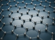
To comprehend why engineers are fervently investigating two-dimensional materials, one must first appreciate the inherent advantages that these materials possess. The quintessential characteristic of 2D materials is their atomic thickness, typically comprising a single or a few layers of atoms. Graphene, perhaps the most renowned of these materials, serves as an exemplar of the extraordinary potential harbored within the flat universe. It boasts remarkable electrical conductivity, mechanical strength, and thermal properties, attributes that are the envy of their three-dimensional counterparts.
Consider the analogy of a piece of paper compared to a book. While the paper may contain a limited expanse of information, it offers a direct interaction that a book cannot replicate in its bulk. Similarly, 2D materials prioritize surface properties over volume characteristics, presenting a unique interactive landscape where quantum effects dominate. Engineers are exploring configurations wherein these ultra-thin materials can unite and orchestrate functionalities unimaginable within the constraints of traditional materials.
Indeed, the realm of 2D materials is expansive. Beyond graphene lie transition metal dichalcogenides (TMDs), black phosphorus, and hexagonal boron nitride, each with its own unique properties and applications. TMDs, for example, have emerged as promising candidates for optoelectronic devices due to their tunable band gaps, which offer versatile capabilities in photodetection and light emission. Such materials can be engineered to respond specifically to certain wavelengths of light, thereby allowing for the development of highly sensitive sensors and advanced photonic devices.
One cannot overlook the structural elegance inherent in 2D materials. The layered architecture presents novel opportunities for heterostructures—combinations of different materials stacked vertically to create synergies that enhance overall performance. Imagine layering flavors in a culinary masterpiece; each ingredient contributes its unique essence to a harmonious finish. In the same vein, engineers fabricate heterostructures from 2D materials to transcend individual limitations, yielding systems that outperform the sum of their parts. The manipulation of electronic transfer between layers can create devices capable of achieving unprecedented efficiency in energy conversion and storage.
This brings us to another compelling aspect of 2D material solutions: scalability. As industries strive to meet ever-growing demands for miniaturization and performance, the synthesis of 2D materials presents a profound solution. These materials can be synthesized through various methods, including chemical vapor deposition (CVD) and liquid exfoliation, both of which lend themselves to large-area production while maintaining the exquisite structural integrity essential for high-performance applications. Thus, engineers are not merely dabbling in theoretical constructs; they are crafting viable solutions for real-world challenges.
However, the journey into the flat dimension is not devoid of tribulations. One of the prevailing challenges in 2D material applications lies in integrating these materials with existing technologies. Engineers must navigate the murky waters between novel material systems and traditional apparatuses, ensuring that the transitions between two-dimensional and three-dimensional realms are seamless. This duality fuels an ongoing dialogue within the engineering community, provoking questions that delve into the intersection of materials science, engineering principles, and practical applications.
Furthermore, the inherent fragility of 2D materials necessitates innovative engineering solutions. Their susceptibility to environmental factors, such as oxidation and humidity, poses a considerable obstacle to their durability and long-term reliability. To combat this vulnerability, engineers are investigating encapsulation techniques, alongside the development of composites that can reinforce the durability of these thin films. Through inventive approaches, they aim to fortify 2D materials, safeguarding their properties while unlocking their full potential.
The sustainability aspect of 2D materials warrants attention as well. In a world where environmental consciousness is paramount, the potential for recycling and utilizing abundant raw materials emerges as a compelling advantage. The methods employed to synthesize these materials often utilize non-toxic precursors and offer avenues for reusability. By marrying nanoscale innovation with eco-friendly practices, engineers can pave the way for a future where 2D materials are not only prevalent in technology but also harmoniously integrated into a sustainable framework.
As we stand on the precipice of an era defined by 2D materials, an exciting narrative unfolds filled with intrigue, innovation, and introspection. The metaphor of climbing a mountain aptly illustrates the engineers’ journey; while the ascent may be challenging, the view from the summit offers breathtaking prospects. As engineers dissect the fabric of these atomically thin solutions and explore their myriad applications, they orchestrate a revolution that transcends conventional barriers and invites the world to re-envision the material landscape.
In conclusion, the exploration of 2D materials encapsulates more than just a fleeting trend in engineering; it represents a profound transformation in how materials can be perceived and utilized. By embracing the flat, engineers are redefining possibilities, forging new paths towards advanced technologies that may one day inform the core of innovations spanning entire industries. As the dialogue surrounding 2D material solutions continues to evolve, the engineering community stands ready, poised to uncover the latent potential embedded within these flat realms, beckoning all to join this exciting journey.