Van der Waals semiconductors represent a fascinating frontier in the realm of condensed matter physics and materials science. Their unique properties arise from the inherent characteristics of their atomic layers, prompting a reevaluation of existing theories regarding semiconductor functionality and performance. This exploration into van der Waals materials is particularly pertinent as the quest for miniaturization and efficiency in electronic devices accelerates.
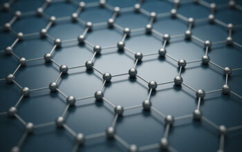
The term “van der Waals semiconductor” refers to a class of materials that exhibit semiconductor properties while being comprised of two-dimensional (2D) atomic structures. Unlike traditional semiconductors, which often rely on covalent bonding phenomena, van der Waals materials leverage weaker van der Waals forces to maintain structural integrity. These forces arise from dipole interactions between electrically neutral atoms, a phenomenon that becomes significantly pronounced in ultra-thin materials.
The anatomy of van der Waals semiconductors typically includes transition metal dichalcogenides (TMDs) such as MoS2, WS2, and WSe2, along with other 2D materials like black phosphorus and graphene. These materials stand out because they can be exfoliated to atomic thickness, enabling vast opportunities for tailoring electronic, optical, and thermal properties. Such exciting possibilities have ignited both theoretical inquiries and experimental endeavors aimed at understanding their underlying physics.
One of the most intriguing attributes of van der Waals semiconductors is their band structure, which is heavily influenced by their dimensionality. In conventional three-dimensional semiconductors, the band gaps are typically sizeable, allowing for efficient electron transport characteristics. However, while TMDs initially present a similar band structure, the reduction to two-dimensionality can lead to a direct bandgap scenario, which is critical for applications in photonics and optoelectronics.
The manifestation of a direct bandgap in materials such as MoS2 transitions van der Waals semiconductors into a new domain of applications, particularly in light-emitting devices and high-efficiency photodetectors. These materials can emit light efficiently at room temperature, a capability that traditional silicon does not possess, thus opening avenues for integrated optoelectronic systems that are more compact and versatile.
Increased understanding of the electronic and optical properties of van der Waals semiconductors has fostered significant interest in defect engineering. The presence of localized states due to imperfections can be exploited to enhance functionalities such as light absorption or photon emission. This concept is underpinned by the ability to strategize the layer compositions of these materials, offering engineered pathways for defect manipulation, which can yield beneficial attributes like increased carrier mobility and modulated bandgaps.
Another compelling aspect of van der Waals semiconductors is their unique mechanical properties. Enabled by their weak interlayer coupling, these materials are not merely fragile; they exhibit exceptional flexibility and resilience. This mechanical robustness, combined with electrical properties, allows for the creation of flexible electronic devices that can withstand significant variations in mechanical stress. The applications of such flexible electronics are manifold, inspiring innovations in wearable technology and portable devices.
Notably, the layered nature of van der Waals materials allows for the potential to construct heterostructures by stacking different 2D materials. This configuration can engender new phenomena such as tunneling, exciton generation, and other quantum effects, which promise to extend the capabilities of layered structures. These heterostructures may serve as the foundation for next-generation transistors, integrated circuits, and quantum computing elements, establishing a pathway toward unprecedented computational efficiencies.
However, the exploration of van der Waals semiconductors extends beyond practical applications and delves into the very essence of condensed matter physics. As researchers unravel the complex interplay of quantum mechanical effects in these materials, it challenges conventional wisdom and invites a rethinking of fundamental principles that govern electronic behavior in low-dimensional systems. The pursuit of a deeper understanding probes into questions of locality, coherence, and frustrated magnetism, bridging gaps between theoretical predictions and experimental observations.
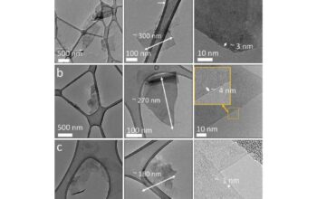
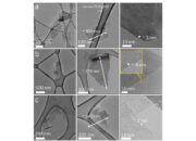
Challenges persist, however. The scalability of these materials for large-scale applications remains a significant hurdle. While the synthesis of single-layer van der Waals semiconductors has been achieved, the reproducibility and uniformity of materials at a larger scale require considerable advancements in production technologies such as chemical vapor deposition (CVD) and liquid-phase exfoliation. Further progress in the synthesis techniques could unlock the full potential of this nascent technology.
In summary, the domain of van der Waals semiconductors encompasses a plethora of fascinating physical phenomena that provoke both scientific inquiry and technological innovation. Their unique structure, compelling band properties, and potential for flexible and multifunctional applications underscore the transformative nature of these materials. As researchers continue to peel back the atomic layers, the implications for future electronic and photonic devices are not only profound but could also represent a monumental shift in how we understand and utilize semiconductor technologies.