In the realm of scientific inquiry, the question of whether one can visualize an atom using visible light occupies a significant position. The vast landscape of atomic structures presents a myriad of complexities that challenge our observational capabilities. In this discourse, we will explore the fundamental principles of light, the limitations imposed by atomic dimensions, the functionality of various microscopy techniques, and the implications of our findings on the understanding of the atomic world.
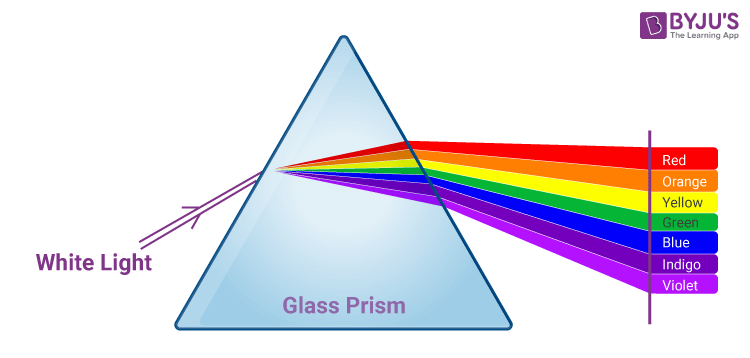
To commence, it is essential to comprehend the nature of visible light itself. Visible light is the segment of the electromagnetic spectrum that is perceptible to the human eye, typically ranging from approximately 400 to 700 nanometers in wavelength. This range includes the colors violet through red and is distinct from other forms of electromagnetic radiation, such as ultraviolet and infrared light. The wavelength of visible light plays a crucial role in dictating the resolution limits of optical imaging techniques.
Atoms, however, exist at an exceedingly diminutive scale, with typical atomic diameters ranging from 0.1 to 0.5 nanometers. This is inherently smaller than the wavelength of visible light. The relationship between the size of the object being observed and the wavelength of the light used for observation is a fundamental principle in optics known as Rayleigh’s criterion. According to this criterion, the ability to resolve two distinct points is contingent upon the wavelength of the light; thus, light with a wavelength larger than the observed object will struggle to produce a discernible image. Consequently, due to their minuscule size, atoms cannot be directly visualized using visible light alone.
Given the constraints posed by the limitations of visible light, one might ponder alternative approaches that scientists have developed over the years to explore atomic and subatomic structures. One such methodology is electron microscopy. This technique employs electrons—subatomic particles that possess significantly shorter wavelengths than visible light—to create images of samples at resolutions that can reach the atomic scale. The advent of transmission electron microscopy (TEM) and scanning electron microscopy (SEM) has revolutionized our ability to visualize atoms indirectly.
In electron microscopy, the de Broglie wavelength of electrons, which is substantially smaller than that of photons in visible light, facilitates the resolution of structures at the nanoscale. TEM, for example, can achieve resolutions on the order of less than 1 angstrom (10 picometers), thus enabling scientists to observe crystalline structures and defects at an atomic resolution. These techniques allow for the probing of materials, elucidating their properties and behaviors at the atomic level, which is paramount for advancements in nanotechnology and materials science.
In addition to electron microscopy, other innovative techniques have surfaced in the scientific domain aimed at imaging and manipulating materials at the atomic scale. Scanning tunneling microscopy (STM) and atomic force microscopy (AFM) stand out as prominent examples. STM utilizes quantum tunneling effects to image surfaces at the atomic level by scanning a conductive tip very close to the surface. This method allows researchers to visualize electronegative distributions and to manipulate individual atoms and molecules, offering unprecedented control over atomic arrangements. On the other hand, AFM relies on the force interactions between a sharp tip and the sample surface to produce high-resolution images, making it a valuable tool in characterizing material properties down to molecular and atomic dimensions.
Another vital dimension of this discussion involves the role of spectroscopic techniques in exploring atomic properties. Although these techniques do not serve to visualize atoms directly, they provide profound insights into the electronic arrangement and interactions of atoms in various materials. Techniques such as X-ray photoelectron spectroscopy (XPS) and nuclear magnetic resonance (NMR) spectroscopy yield considerable information about electronic states, chemical bonding, and molecular dynamics, enhancing our understanding of atomic behavior within macroscopic materials.
While it is clear that direct observation of atoms with visible light remains an unattainable feat, the methodological robustness of contemporary physics equips researchers with formidable tools capable of indirect observation, characterization, and manipulation of atomic structures. These methods have broadened our comprehension of the atomic world that underpins all matter, elucidating phenomena from chemical reactions to the stability of materials.
Additionally, the implications of our inability to see atoms directly with visible light resonate deeply within the broader scientific community. The necessity for advanced imaging techniques indicates the profound complexity inherent in atomic structures and interactions. It emphasizes the importance of interdisciplinary approaches that blend classical physics, materials science, and advanced imaging technology. As research endeavors continue to progress, the quest for further understanding at atomic scales stands as a testament to human ingenuity and ambition in unveiling the intricacies of our universe.
In conclusion, while the limitations of visible light preclude direct observation of atomic structures, the scientific community has cultivated a plethora of alternatives that enrich our understanding. The exploration of atoms, while inherently perplexing, is met with significant progress through various advanced microscopy techniques and spectroscopic analyses. Ultimately, the ongoing quest for elucidating the atomic tapestry that governs matter continues to inspire profound discoveries and innovations across multiple scientific disciplines.


