Short Answer
Definition of Doping in Materials Science
Doping refers to the intentional introduction of impurities into a pure material, typically a semiconductor, to modify its electrical properties. This process transforms an otherwise insulating or weakly conductive solid into a material capable of efficiently conducting electricity. By altering the electronic structure of the host material, doping enables the creation of semiconductors that are fundamental to modern electronic devices.
Fundamentals of Solid-State Structure
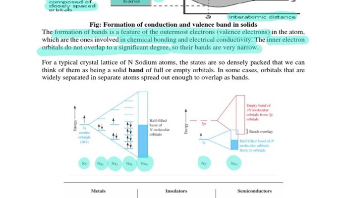
At the microscopic level, solids are composed of atoms arranged in a regular lattice. The electrons in these atoms occupy discrete energy levels, which determine the material’s electrical behavior. In undoped semiconductors, electrons reside primarily in the valence band, while the conduction band above remains largely unoccupied. The energy difference between these two bands, known as the band gap, dictates the energy required for electrons to move freely and conduct electricity.
Mechanism of Doping
Introducing impurities into a semiconductor alters its electronic band structure by adding extra electrons or creating vacancies known as holes. These changes effectively modify the band gap and introduce new energy states within it, thereby enhancing the material’s conductivity. The process can either increase the number of free electrons or holes, depending on the type of dopant used.
Types of Doping
- N-type Doping:
This involves adding donor atoms, such as phosphorus, which have more valence electrons than the host semiconductor (e.g., silicon). These extra electrons occupy energy levels just below the conduction band, increasing the electron concentration and improving electrical conductivity. - P-type Doping:
In this case, acceptor atoms like boron, which have fewer valence electrons, are introduced. These create holes in the valence band, allowing electrons to move and effectively increasing hole concentration. Electrical conduction occurs through the movement of these holes.
Impact of Doping on Semiconductor Properties
The electrical characteristics of semiconductors can be dramatically enhanced through doping. For instance, pure silicon exhibits limited conductivity at room temperature, but doping can increase its conductivity by several orders of magnitude. This principle underlies the operation of essential electronic components such as diodes and transistors, which form the foundation of digital technology.
However, the effectiveness of doping depends on several factors including dopant concentration, temperature during doping, and the crystallographic orientation of the host material. Precise doping techniques like ion implantation and diffusion are critical to achieving the desired electrical properties.
Temperature Effects on Doped Semiconductors
The relationship between temperature and conductivity in doped semiconductors is complex. Generally, conductivity increases with temperature as more charge carriers gain sufficient energy to move freely. Yet, beyond certain temperature thresholds, increased thermal vibrations cause scattering of these carriers, reducing mobility and thus conductivity. This interplay necessitates careful optimization of doping levels and operating conditions for specific applications.
Doping in Advanced Materials
Beyond traditional semiconductors, doping plays a pivotal role in emerging materials such as graphene and transition metal dichalcogenides (TMDs). These two-dimensional materials possess exceptional electronic, optical, and mechanical properties. Doping can tailor their electrical and optical behavior, opening new possibilities for next-generation electronic and photonic devices. Understanding how doping principles apply to these novel materials remains an active area of research.
Challenges and Innovations in High-Level Doping
While increasing dopant concentration can enhance conductivity, excessive impurities may lead to adverse effects such as charge carrier scattering and structural degradation, ultimately limiting performance. Researchers are exploring innovative doping methods to overcome these challenges, aiming to maximize conductivity without compromising material integrity.
Techniques like self-assembly and molecular beam epitaxy offer precise control over dopant placement and concentration. These advanced methods hold promise for fabricating materials with finely tuned properties, potentially revolutionizing semiconductor technology.
Significance of Doping in Technology and Science
Doping is a cornerstone of modern electronics, enabling the transformation of ordinary solids into highly conductive materials essential for countless devices. Its influence spans multiple disciplines, bridging chemistry and physics to manipulate electronic properties at the atomic level. Continued advancements in doping techniques are vital for the development of more efficient, powerful, and versatile technologies, underscoring its enduring importance in science and industry.
FAQ
What is doping in materials science?
Doping is the deliberate introduction of impurities into a solid to modify its electrical properties, often to increase conductivity.
What are n-type and p-type doping?
N-type doping adds atoms that donate extra electrons, enhancing electron conduction, while p-type doping adds atoms that create holes, facilitating hole conduction.
How does doping improve semiconductor performance?
By adjusting electron and hole concentrations, doping enables control over conductivity and the electrical characteristics necessary for device functionality.
What challenges exist with doping at high concentrations?
Excessive doping can cause charge carrier scattering and material degradation, reducing overall conductivity and device reliability.
Are doping techniques evolving for new materials?
Yes, emerging techniques like self-assembly and molecular beam epitaxy aim to control dopant distribution precisely, especially in novel materials like graphene and TMDs.


Leave a Reply