Short Answer
Definition of Two-Dimensional (2D) Materials
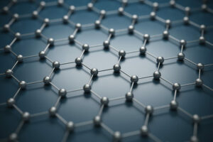
Two-dimensional materials are crystalline solids characterized by their atomic-scale thickness, typically consisting of a single or few layers of atoms arranged in a planar structure. Unlike traditional crystals that extend their periodic atomic arrangement in three dimensions, 2D materials exhibit order primarily within a two-dimensional plane, resulting in unique physical and chemical properties.
- Crystals:
Traditionally, crystals are solids with atoms, molecules, or ions arranged in a repetitive, three-dimensional lattice. - 2D Materials:
These are materials with reduced dimensionality, where the crystal lattice extends predominantly in two dimensions, often just one or a few atomic layers thick.
Historical Context and Notable Examples
The discovery of graphene, a monolayer of carbon atoms arranged in a hexagonal lattice, marked a pivotal moment in materials science. Graphene’s exceptional electrical conductivity, mechanical strength, and thermal properties have spurred extensive research into other 2D materials. Following graphene, transition metal dichalcogenides (TMDs) such as molybdenum disulfide (MoS2) and tungsten diselenide (WSe2) have gained prominence due to their semiconducting properties and potential for optoelectronic applications.
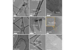
Structural Characteristics and Synthesis Methods
2D materials are typically derived from bulk layered crystals by isolating individual atomic layers. Several techniques enable this process:
- Mechanical Exfoliation:
Physically peeling layers from bulk crystals, often using adhesive tapes, to obtain thin sheets. - Chemical Vapor Deposition (CVD):
A scalable method where gaseous precursors react on substrates to form continuous 2D layers. - Liquid Phase Exfoliation:
Using solvents and ultrasonic energy to separate layers into dispersions of 2D flakes.
Physical and Electronic Properties of 2D Materials
The reduced dimensionality of 2D materials profoundly influences their electronic, optical, and mechanical behaviors. Quantum confinement effects modify their band structures, often resulting in enhanced electron mobility and conductivity compared to their bulk counterparts. For example, graphene exhibits near-ballistic electron transport, while monolayer TMDs display direct bandgaps, making them suitable for optoelectronic devices.
Quantum Confinement and Band Structure
When the thickness of a material approaches the atomic scale, electrons become confined in the perpendicular direction, altering energy levels and band structures. This leads to phenomena such as:
- Transition from indirect to direct bandgap in monolayer TMDs.
- Enhanced electrical conductivity and carrier mobility in graphene.
Optical Properties and Layer Dependence
The interaction of 2D materials with light varies significantly with the number of layers. Monolayer TMDs exhibit strong photoluminescence due to their direct bandgap, whereas multilayer forms tend to have indirect bandgaps, reducing optical emission efficiency. This tunability is critical for applications in photodetectors, light-emitting diodes, and solar cells.
Transition Metal Dichalcogenides (TMDs): A Closer Look
TMDs are a family of layered compounds with the general formula MX2, where M represents a transition metal (e.g., Mo, W) and X is a chalcogen (e.g., S, Se). These materials exhibit diverse electronic phases ranging from semiconducting to metallic and even superconducting states. Their ability to form heterostructures by stacking different 2D layers enables the engineering of novel electronic and optical functionalities.
Applications and Technological Implications
2D materials hold promise for revolutionizing various technological sectors due to their exceptional properties:
- Flexible Electronics:
Ultra-thin and bendable devices that maintain performance under mechanical strain. - Transparent Conductors:
Materials that combine electrical conductivity with optical transparency for displays and solar cells. - Quantum Devices:
Exploiting quantum phenomena in 2D materials for next-generation computing and sensing.
Challenges in Industrial Scale-Up and Integration
Despite their potential, several obstacles hinder the widespread commercial adoption of 2D materials:
- Scalability:
Mechanical exfoliation is limited to small-scale production, while CVD requires precise control over growth parameters to ensure uniformity and quality. - Material Purity:
Defects and impurities can degrade the performance of 2D materials, necessitating advanced synthesis and purification techniques. - Integration:
Incorporating 2D materials into existing semiconductor manufacturing processes remains complex.
Theoretical Insights and Surface Phenomena
The unique surface-dominated nature of 2D materials leads to complex interactions that influence their properties. Key areas of ongoing research include:
- Electron-phonon coupling effects impacting electrical and thermal transport.
- Role of surface defects and their influence on electronic behavior.
- Modulation of properties by external stimuli such as strain, temperature, and electromagnetic fields.
Why Two-Dimensional Materials Are Transformative
The study and application of 2D materials represent a frontier in material science with far-reaching implications. Their distinctive properties enable advancements in electronics, photonics, and energy technologies, potentially leading to devices that are smaller, faster, more efficient, and flexible. As research progresses, these materials are poised to redefine the capabilities of modern technology and open new avenues for scientific discovery.
FAQ
What are 2D materials?
2D materials are crystalline solids consisting of a single or few layers of atoms, exhibiting unique physical and chemical properties.
What is graphene?
Graphene is a single layer of carbon atoms arranged in a hexagonal lattice, known for its exceptional electrical conductivity and mechanical strength.
What are transition metal dichalcogenides (TMDs)?
TMDs are layered compounds with diverse electronic phases, exhibiting properties that range from semiconducting to superconducting.


Leave a Reply