Short Answer
Definition of Two-Dimensional Materials
Two-dimensional (2D) materials are a class of substances defined by their atomic-scale thickness, typically consisting of just one or two layers of atoms, while extending extensively in the other two spatial dimensions. This extreme thinness imparts them with distinctive physical and chemical properties that differ markedly from their bulk counterparts.
- Atomic Thickness:
2D materials are essentially one or two atoms thick, making them the thinnest possible materials. - Extended Planar Dimensions:
Despite their minimal thickness, these materials can span large areas in the other two dimensions. - Unique Properties:
Their reduced dimensionality leads to novel electrical, mechanical, thermal, and optical behaviors.
Historical Context and Key Examples
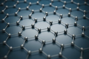
The discovery of graphene, a single layer of carbon atoms arranged in a hexagonal lattice, marked the inception of intense research into 2D materials. Graphene’s exceptional electrical conductivity, mechanical strength, and thermal properties have made it a benchmark for this field. Beyond graphene, other significant 2D materials include transition metal dichalcogenides (TMDs), hexagonal boron nitride (h-BN), and black phosphorus, each bringing unique functionalities to the table.
Notable 2D Materials
- Graphene:
Known for its outstanding conductivity and strength, it has revolutionized materials science. - Transition Metal Dichalcogenides (TMDs):
Semiconducting materials whose electronic properties can be tuned by adjusting layer thickness, useful in flexible electronics and photonics. - Hexagonal Boron Nitride (h-BN):
An insulating material with excellent thermal stability and biocompatibility. - Black Phosphorus:
Exhibits promising electronic characteristics but is sensitive to environmental degradation.
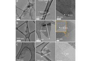
Synthesis Techniques and Challenges
Producing high-quality 2D materials at scale remains a significant hurdle. Two primary methods dominate the synthesis landscape:
- Mechanical Exfoliation:
This technique involves peeling layers from bulk crystals, yielding high-quality but small-sized flakes, limiting scalability. - Chemical Vapor Deposition (CVD):
Enables the growth of continuous thin films over large areas but can introduce defects and impurities that degrade material performance.
Ensuring uniformity, purity, and defect control during synthesis is critical for practical applications, yet remains a complex challenge.
Stability and Environmental Sensitivity
Many 2D materials are prone to degradation when exposed to ambient conditions such as air, moisture, or elevated temperatures. For example, black phosphorus rapidly oxidizes in air, necessitating protective encapsulation to maintain its electronic properties. Researchers are actively exploring hybrid structures combining 2D materials with traditional substrates to enhance stability and extend their functional lifespan.
Applications in Energy Technologies
The exceptional electrical conductivity and surface area of 2D materials make them promising candidates for next-generation energy storage devices. Their integration into batteries and supercapacitors could significantly improve charge capacity, charging speed, and overall energy efficiency.
- Electrodes:
2D materials can serve as high-performance electrodes, enhancing charge transport and storage. - Energy Efficiency:
Their unique properties may lead to devices with faster charging times and longer lifespans.
However, the complexity of manufacturing and integrating these materials into commercial energy solutions remains a critical consideration.
Role in Quantum Computing
Certain 2D materials, including graphene and some TMDs, exhibit properties conducive to quantum phenomena such as topological insulation. These characteristics position them as promising materials for developing qubits, the fundamental units of quantum computers. Despite theoretical potential, practical challenges such as maintaining qubit stability and minimizing decoherence times continue to impede progress toward viable quantum computing devices.
Biomedical Implications
2D materials are increasingly explored for biomedical applications due to their biocompatibility and surface chemistry. For instance, hexagonal boron nitride is being investigated for drug delivery systems and biosensors. Nonetheless, ethical considerations and regulatory frameworks must be carefully addressed to ensure patient safety and responsible deployment of nanomaterials in clinical environments.
Engineering Innovations: Heterostructures and Beyond
A remarkable feature of 2D materials is their ability to be stacked into heterostructures-layered assemblies of different 2D materials that create new functionalities unattainable by individual layers alone. This capability enables the design of devices with customized electronic band gaps, paving the way for breakthroughs in optoelectronics, photodetection, and flexible display technologies.
Environmental and Sustainability Considerations
As the production of 2D materials scales up, environmental impact and sustainability become critical concerns. Responsible sourcing of raw materials, minimizing waste, and developing recyclable processes are essential to ensure that the advancement of 2D materials aligns with ecological stewardship.
Summary and Future Outlook
Two-dimensional materials represent a frontier of scientific and technological innovation, offering unprecedented properties and applications across diverse fields. While their potential is vast-from energy storage and quantum computing to biomedicine and flexible electronics-the challenges of synthesis, stability, scalability, and environmental responsibility require coordinated efforts among scientists, engineers, and policymakers. The journey toward fully harnessing 2D materials is complex but holds the promise of transformative breakthroughs that could redefine multiple industries.
FAQ
What are 2D materials?
2D materials are materials that are only one or two atoms thick, offering unique physical and chemical properties different from their bulk equivalents.
Why is graphene important among 2D materials?
Graphene was the first isolated 2D material and is known for its exceptional electrical and mechanical properties, sparking extensive research in the field.
How are 2D materials produced?
They are commonly produced by mechanical exfoliation, which peels layers from bulk crystals, or by chemical vapor deposition, which grows thin films on substrates.
What industries could benefit from 2D materials?
Electronics, energy storage, quantum computing, photonics, and biomedical fields are all potential beneficiaries of 2D material technologies.
What limits the widespread use of 2D materials?
Challenges include difficulty in producing large-scale high-quality materials, stability under normal conditions, and integration challenges in device fabrication.


Leave a Reply