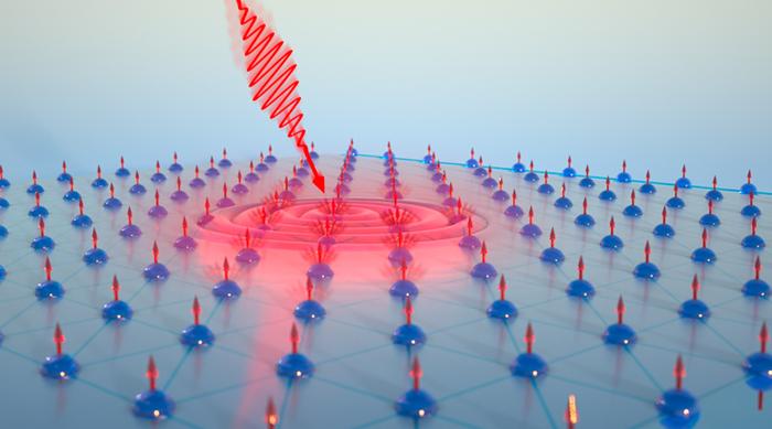
The advancement of photonics technology has garnered significant attention in recent years, particularly concerning the enhancement of data transmission and processing capabilities. Among the myriad of innovations, the incorporation of insulating materials—referred to here as “buffers”—promises to propel the efficiency of optical circuits to unprecedented levels. This discourse explores the dynamics of buffer materials in photonics, shedding light on their roles in optimizing performance and understanding the underlying principles at work.
To fully appreciate the implications of buffer materials, one must recognize the fundamental challenges associated with optical memory devices and circuits. Traditional photonic devices, reliant on either semiconductor or dielectric materials, have long grappled with limitations in speed, capacity, and energy consumption. The integration of buffer materials introduces a promising solution that not only ameliorates these constraints but also catalyzes a paradigm shift in optical circuit design.
At the core of this transformation is the insulator’s propensity to enhance optical memory device efficiency dramatically. Insulators possess unique properties that allow for the manipulation and control of light at a microscopic level. By serving as a critical intermediary, buffer materials can effectively mitigate loss of signal, optimize bandwidth, and increase the fidelity of data transmission. This functionality is paramount in contemporary applications where high-capacity and high-speed data processing are non-negotiable requirements.
The enhancement in efficiency can be attributed to several factors inherent in the physical properties of the insulating materials. For instance, the low absorption coefficients of certain insulators enable prolonged light propagation without substantial energy dissipation. Additionally, the elevated refractive index contrast between the buffer and the active optical components facilitates better confinement of light—thereby reducing scattering losses and augmenting the overall signal quality.
Moreover, the utilization of insulator materials opens avenues for novel designs in optical circuits, as it allows for greater material flexibility. Researchers have begun to explore a range of materials including tantalum pentoxide and silicon dioxide, which present advantageous thermal and optical characteristics. These materials can be engineered to match specific operational scenarios, thus broadening the spectrum of potential applications from telecommunications to quantum computing.
Decomposing the observed synergy between buffer materials and optical efficiency reveals deeper insights into the physical interactions at play. The utilization of buffer layers stabilizes optical pathways through multiple scattering mechanisms which can occur in practical implementations, where structural imperfections frequently perturb light propagation. By creating a uniform medium wherein light can travel more freely, buffers serve to bolster the effectiveness of photonic integrated circuits (PICs).
This phenomenon invites further investigation into the interactions between light and various material properties on a quantum level. In this realm, advanced modeling techniques, such as finite element analysis and optical simulation software, can predict the nuanced behaviors of light in response to different material configurations. Exploring these interactions further enriches our understanding of the optical landscape and its myriad implications for technological advancement.
Aside from the propagation-related advantages, the thermal stability of insulator materials cannot be overlooked. Buffer layers can enhance the thermal management of optical devices, ensuring that operational efficiency is maintained under varied environmental conditions. This characteristic is particularly beneficial in high-power applications, where excessive heating can degrade performance and reliability.
Further, the promise of scalability cannot be ignored. The integration of efficient buffer materials paves the way for the miniaturization of optical circuits. As devices become smaller and more compact, their efficiency remains paramount. This innovation dovetails harmoniously with the existing trends toward miniaturized electronics and systems-on-a-chip. To this end, buffer materials not only serve a functional purpose but also embody the vision of the future: small, fast, and energy-efficient optical devices.
Looking forward, it is essential to address some of the inherent challenges associated with the implementation of insulating buffers. For instance, interface quality between the buffer and the active material can significantly affect device performance. Advanced fabrication techniques that minimize defects and ensure atomic-level precision will be imperative to ensuring the full potential of these materials is realized.
Moreover, as innovations in material science continue to emerge, there exists a necessity for rapid prototyping and testing methodologies that can keep pace with the increasingly complex demands of photonic applications. Future research must cultivate interdisciplinary collaboration between physicists, materials scientists, and engineers. Such collaborative endeavors are crucial to unlocking new material combinations and optimizing existing solutions.
In conclusion, the incorporation of buffer materials into optical circuits marks a pivotal advancement in the field of photonics. The attributes of these insulators present an array of opportunities that extend beyond mere efficiency gains. As research continues to uncover the intricate dynamics of light-matter interactions, we stand on the brink of a new era in optical technology. Enhanced optical circuits, driven by innovative insulator materials, promise not only to advance current technologies but also to forge new pathways toward unexplored realms of information processing and data transmission.


